

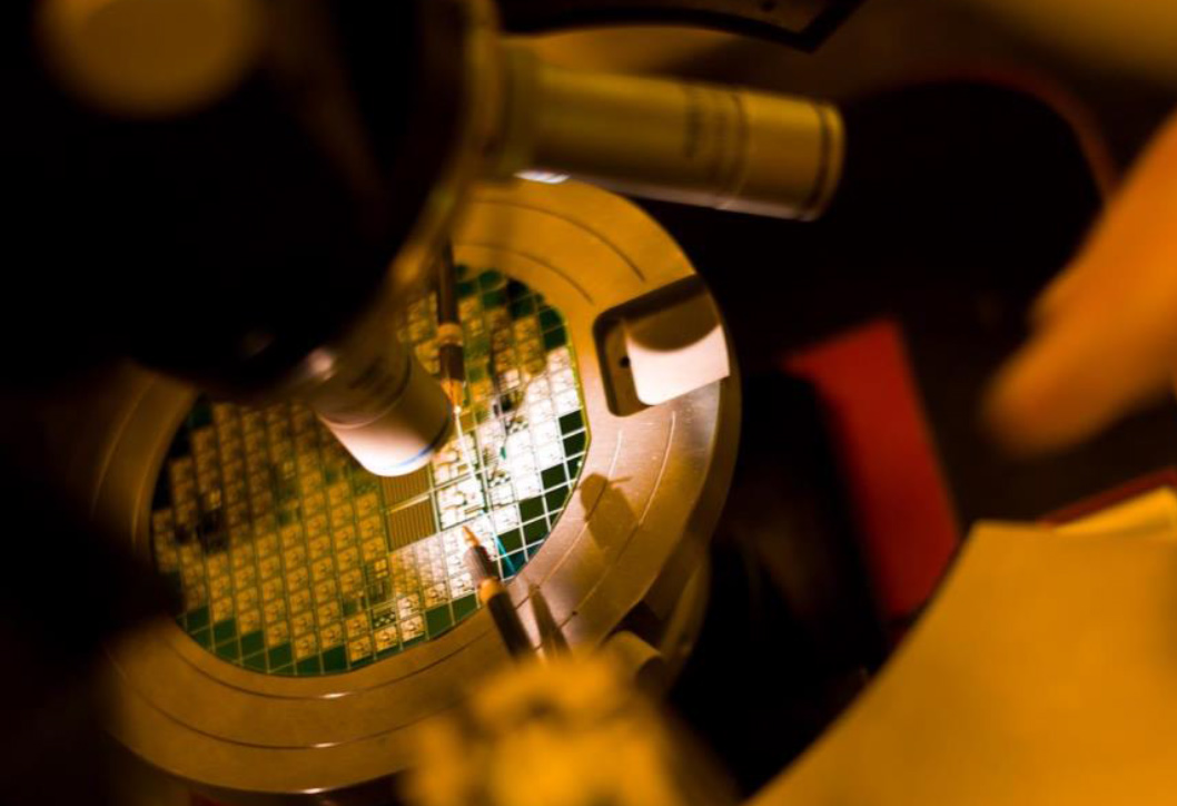
GlobalFoundries has revealed additional details regarding its 22nm fully-depleted silicon-on-insulator (FD-SOI) fabrication technology. The manufacturing process will be ready for tape-outs in early 2016 and will be used for mass production of chips by late next year. While the tech has a number of advantages, the process is designed primarily for small high-volume chips and designers of larger ICs will hardly be interested in using it.
“We are developing 22nm FD-SOI process technology right now,” said Gerd Teepe, director and design engineering at GlobalFoundries, reports EETimes. “The plan is to qualify the process by early 2016 and start volume production by the end of 2016.”
GlobalFoundries 22nm FD-SOI will use back-end-of-line (BEOL) interconnect flow of STMicroelectronics’ 28nm FD-SOI as well as front-end of line (FEOL) of STM’s 14nm FD-SOI. Just like two aforementioned process technologies from STM, GlobalFoundries’ 22nm FD-SOI is a planar technology with fewer metal layers and mask steps compared to fabrication processes, which use FinFET transistors. However, unlike STM’s 14nm FD-SOI, the new tech from GlobalFoundries does not require double-patterning anywhere, which simplifies chip design.
“We are using STMicroelectronics’ 14nm FD-SOI in our frontend, while using 28nm FD-SOI in the backend,” explained Mr. Teepe.
Since the 22nm FD-SOI relies on a 28nm BEOL, die sizes of chips produced using the technology will be similar to those made using 28nm nodes. As a result, it will not make a lot of sense for makers of large chips to transit to 22nm FD-SOI since they will increase their costs (FD-SOI wafers are more expensive than bulk wafers), but will not be able to introduce a lot of new features without considerably increasing their die sizes (which increases costs further). For makers of smaller high-volume ICs [integrated circuits] it makes considerably more sense to adopt 22nm FD-SOI since they keep their design costs and power consumption low, but will be able to increase performance.
Initially, GlobalFoundries will address its existing SOI customers with the technology, but eventually the tech and its successors may become economically feasible and will be offered to designers of chips for wearable and Internet-of-Things devices.
“We hope to be able to leverage FD-SOI’s super low-power strategy for wearables and other products, whose volume will start to emerge by then,” said Mr. Teepe.
GlobalFoundries’ 22nm FD-SOI is compatible with neither 14nm nor 28nm FD-SOI, hence, customers to STMicroelectronics and Samsung Foundry (which licenses 28nm FD-SOI from STM) will have to re-implement their chips for the new process.
Discuss on our Facebook page, HERE.
KitGuru Says: While GF’s 22nm FD-SOI looks like a solution for very specific chips and customers, it generally looks like the company is a tad late with it. The technology will hardly be used by Advanced Micro Devices, GlobalFoundries’ largest customer, as well as makers of advanced system-on-chips for leading-edge mobile devices. GlobalFoundries should have offered the process several year ago.
