

It is not a secret that transitions to newer chip manufacturing processes are getting more difficult from financial capital standpoint since not only research and development costs more than before, but also production equipment is getting more expensive. In a bid to keep their prices at current levels, semiconductor companies need to increase transistor densities of their process technologies at a pace faster than Moore’s law. Intel believes that it can do this at 7nm and 10nm.

According to some estimates, it costs $1.3 – $1.5 billion to create a new manufacturing process from scratch nowadays, which involves a lot of fundamental research as well as development of new materials. In addition, large makers of semiconductors sometimes also participate in development of production equipment. Once fabrication technology is developed, manufacturers need to equip their fab(s) with new tools or even build new a new fab. As a result, it requires tremendous amount of capital to start making new chips using a new process technology.
“Capital intensity is going to go up as measured by capital cost per square inch of silicon,” said Stacy Smith, chief financial officer of Intel, during the company’s quarterly conference call with investors and financial analysts.
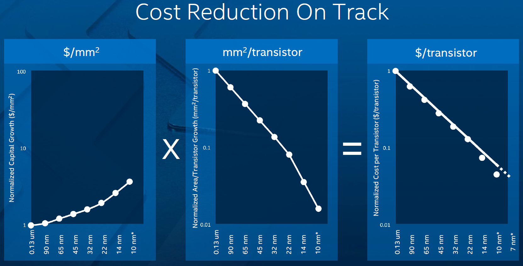
That capital cost is a headache for all makers of chips because if it is too high, they either need to lower their margins or increase their prices. To offset increases of capital costs per square millimeter of a chip, makers of semiconductors need to increase transistor densitires, which is not an easy task due to leakages and other effects. However, Intel claims that it has found ways to increase those densities going forward, which will make its 7nm and 10nm process technologies economically feasible.
“We believe that through 14nm, 10nm and with some insight all the way down the 7nm we can offset that increase in capital cost per square inch of silicon by improving our density,” said Mr. Smith. “So we can keep the cost per transistor coming down at the historical curve.”
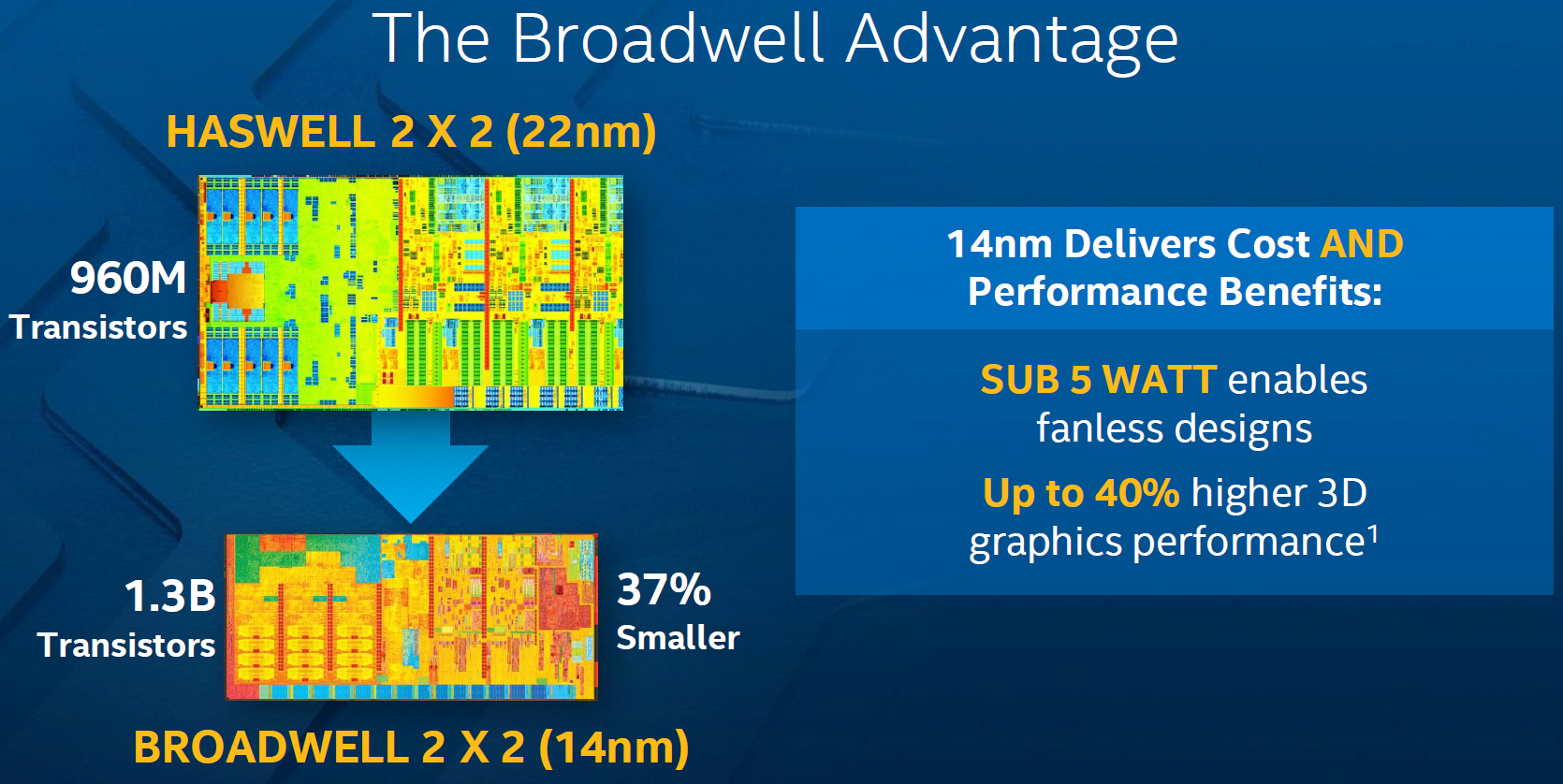
Increasing transistor density helps Intel to reduce die sizes of its chips without decreasing their performance or feature-set. For example, Intel's dual-core “Broadwell” processor is 37 per cent smaller than comparable “Haswell” chip, but its feature sizes are 33 per cent smaller, which is a good example how transistor density increases from generation to generation. As a result, increase of transistor density is a crucially important thing for the company in the future.
“We believe [that on] the 10nm [node] the capital per wafer start does go up, but it goes up less than the density does,” said Brian Krzanich, chief executive officer of Intel. He added that the company’s 10nm unit costs and per-transistor costs will offset increased capital requirements.
Discuss on our Facebook page, HERE.
KitGuru Says: Keeping in mind that Intel controls architecture, design, technology and manufacturing aspects of its business, the company has a lot of flexibility. In general, Intel can make almost any reasonably good manufacturing process economically feasible for itself. Still, the chip giant has to solve numerous fundamental technology-related challenges, such as materials, leakage and so on.