
In a bid to convince its partners and investors that it is on-track with its Tick-Tock strategy, Intel Corp. reportedly plans to showcase several yet-unannounced products at the Intel Developer Forum event this September. While the company will demonstrate certain new things, it does not mean that everything goes truly smoothly.
Intel is set to showcase its 14nm processors and also unveil its first wafers processed using 10nm manufacturing technology at its developer forum in San Francisco, California, in September, reports DigiTimes. The move is supposed to showcase Intel’s investors and partners that despite of problems the company has faced with its 14nm process technology it is still about two years away from 10nm production (which means that the Tick-Tock works) and months away from commercial launch of the first 14nm chips.
The web-site did not elaborate which microprocessors made using 14nm manufacturing technology Intel will showcase. The world’s largest chipmaker already demonstrated its code-named “Broadwell” chips in action at IDF 2013 almost a year ago. It is logical to assume that this year the company will demonstrate central processing units based on the Skylake micro-architecture due in the second quarter next year (according to unofficial information).
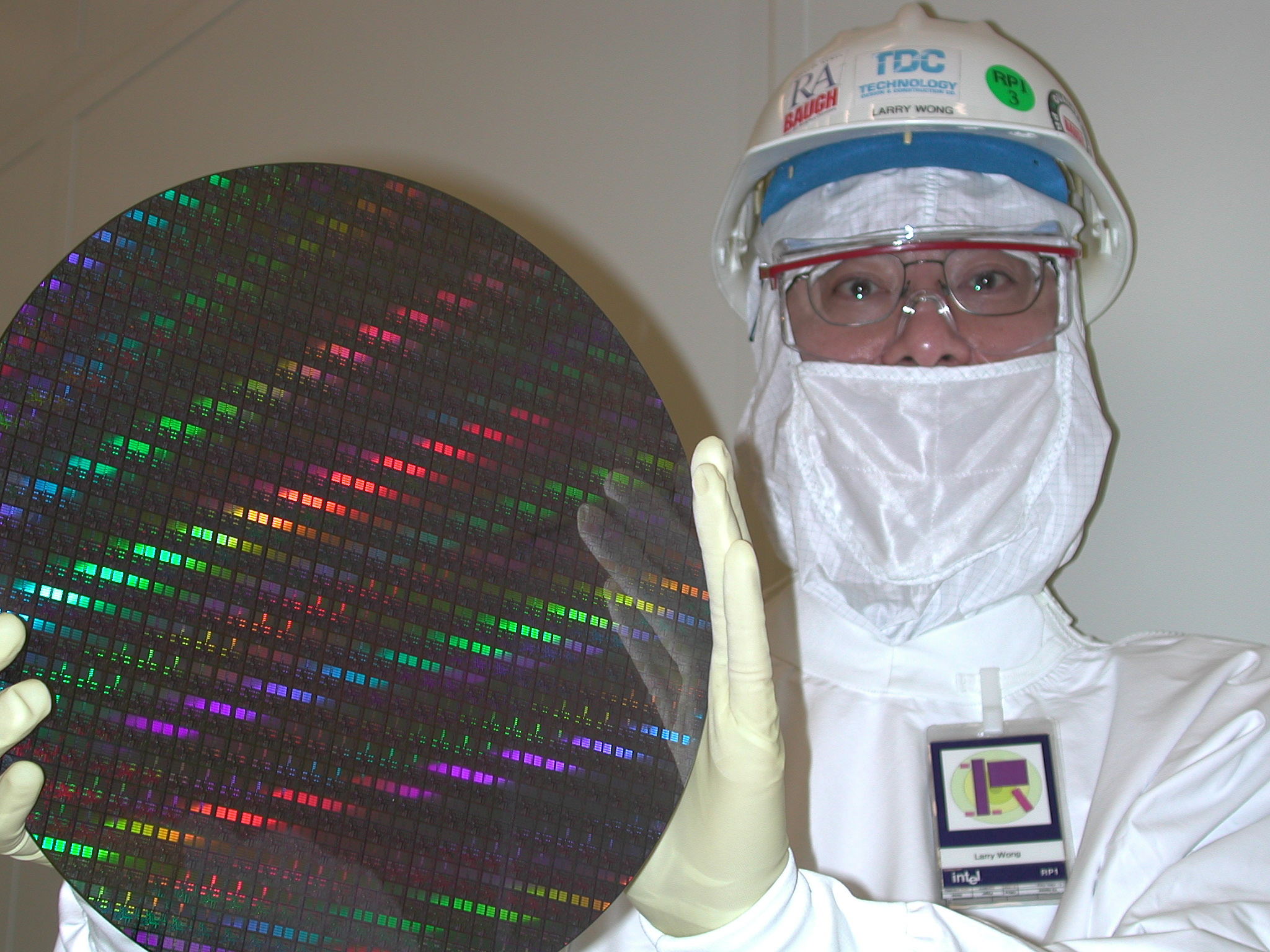
So far Intel has never demonstrated any wafers processed using 10nm manufacturing technology. The company also has not revealed almost any peculiarities regarding the fabrication process too.
What is pretty guaranteed is that Intel’s 10nm process technology will not take advantage of extreme ultraviolet lithography (EUV) since it is unlikely that ASML or Nikon, two major producers of semiconductor manufacturing equipment, will be able to supply enough EUV scanners by 2016, when Intel plans to start mass production of 10nm chips. Since EUV seems to be too late for 10nm, Intel will use a tricky multi-patterning approach to produce chips with 10nm feature sizes. Multi-patterning (quad-patterning, according to rumours regarding Intel’s 10nm fabrication process) is a rather expensive and time-consuming semiconductor manufacturing technology.
It will be interesting to see what kind of 10nm wafer Intel will reveal. Traditionally, chip-makers show off wafers with SRAM memory cells in a bid to demonstrate readiness of the manufacturing process. However, given the fact that the 10nm chips code-named Cannonlake or Airlake are just two years away from mass production (at least, based on expectations), Intel could demonstrate wafers with its next-gen design(s) at the IDF 2014.
Intel did not comment on the news-story.
Discuss on our Facebook page, HERE.
KitGuru Says: While the Skylake demonstration is an interesting event as it will reveal where Intel is going in terms of micro-architecture (or, it will show what Intel wants to show), the unveiling of the 10nm process technology will be much more important as it will uncover not only Intel’s plans and challenges, but plans and challenges of the whole semiconductor industry.