

Intel Corp. has implied a number of times that it did not need to use extreme ultraviolet lithography for its 7nm manufacturing process. However, after facing problems with multi-patterning methods at 14nm and 10nm fabrication technologies, it seems that the company has changed its mind. This week Intel said that it is exploring possibilities to use EUV at 7nm. Unfortunately, it is still unclear whether appropriate tools will be ready by the time Intel needs them.
“At 7nm, we are trying to bring in EUV,” said Stacy Smith, chief financial officer of Intel, during the company’s quarterly conference call with investors and financial analysts. “Depending on the health of that [technology], we could be at two years, we could be at 2.5 years [with 10nm fabrication process].”
Extreme ultraviolet lithography is an advanced patterning technology that allows semiconductor makers to keep scaling down feature sizes of chips. Thanks to 13.5nm wavelength of EUV lasers, it will be possible to “draw” finer elements of chips without using difficult multiple-patterning techniques and implementing additional metal layers that complicate manufacturing technology and make it more expensive. EUV is also expected to bring significant benefits in terms of yield and cycle time.

Intel has been using various forms of multiple-patterning, a semiconductor manufacturing technology that allows to enhance feature density by drawing multiple lines on the same photoresist layer using different photomasks, since its 65nm process technology. While in general usage of multi-patterning has not been a problem for Intel, things got very complicated at 14nm, when the number of mask steps increased. In a bid to ensure that it can produce chips using 10nm fabrication technology with high yields and in high volume, Intel decided to postpone the roll-out of appropriate chips by one year to tune the manufacturing process and its designs. Some believe that Intel plans to use quintuple-patterning for its 10nm tech, which is extremely complex and expensive.
Because of extreme difficulties it faces with modern process technologies, Intel indicated that from now on it will produce three generations of chips using the same process technology instead of two. The company said that it would like to get back to two-year cycle time and that it could be possible with EUV lithography.
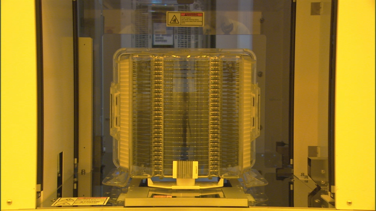
While EUV scanners have existed for years, their productivity is too low for commercial production. Experimental ASML NXE:3300B EUV scanners are capable of processing 500 wafers per 24 hours. However, for high-volume manufacturing wafer scanners should process 1500+ wafers per 24 hours. It is still unclear when EUV scanners from ASML be able to hit necessary production capabilities.
“We will take a look at what is the maturity of EUV, what is the maturity of the material science changes that are occurring, what is the complexity of the product roadmap that we are adding, and make that [cycle-related] adjustment in the future,” said Brian Krzanich, chief executive officer of Intel.
Discuss on our Facebook page, HERE.
KitGuru Says: Since it is believed that Intel has ordered 15 EUV scanners from ASML earlier this year, it looks like there is a plan to start using EUV at 7nm several years after 10nm introduction in 2017. Depending on capabilities of the tools, Intel may start making 7nm chips in 2019 or 2020.