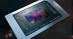

Intel Corp. officially confirmed on Wednesday that it will not use extreme ultraviolet (EUV) lithography for its 10nm process technology allegedly due to come online in 2016. Apparently, not only the EUV scanners are not ready, but backbones of certain fabs may not support the new equipment due to its dimensions.
“We know we can get through 10nm without EUV,” said Brian Krzanich, chief executive officer of Intel at the Citi Global Technology Conference.
While it was expected by virtually all industry analysts that Intel would not use extreme ultraviolet lithography for 10nm node, this is the first time when Intel officially confirmed this.
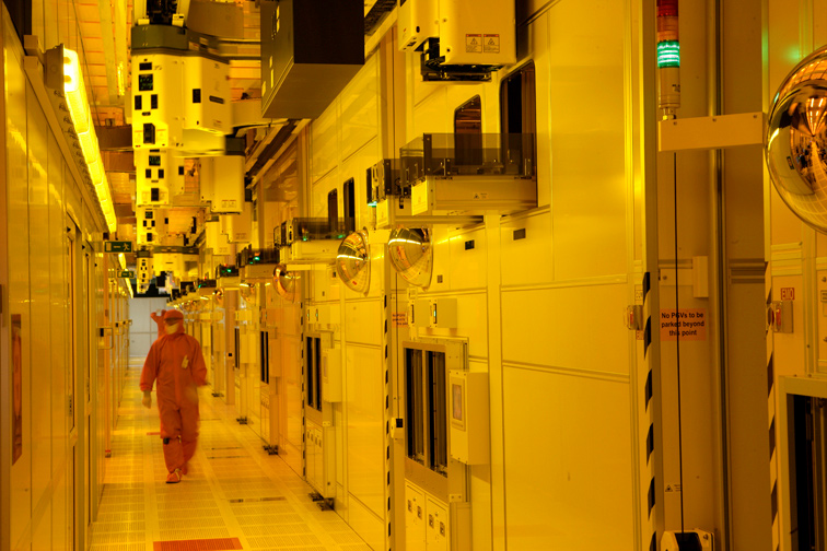
Inside Intel's fab in Ireland
Both ASML and Nikon, two major producers of semiconductor manufacturing equipment, will be able to supply enough EUV scanners by 2016, when Intel presumably plans to start mass production of 10nm chips. Since EUV is too late for 10nm, Intel will use a tricky multi-patterning approach to produce chips with 10nm feature sizes. Multi-patterning (quad-patterning, according to rumours regarding Intel’s 10nm fabrication process) is a rather expensive and time-consuming semiconductor manufacturing technology.
“We are late with EUV […] and technologies needed for it,” admitted Mr. Krzanich.
Intel's fab in Ireland
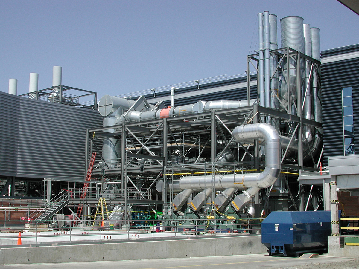
The EUV scanners are only a part of the problem. The tools require a lot of other equipment to function and it is unclear whether these machines are ready. Moreover, the backbone tools for EUV scanners are going to be larger than today’s, which means that they may not fit into all current fabs (many of which were not designed for EUV equipment from the start).
“What you always have to remember with fab equipment is kind of like an iceberg,” explained the head of Intel. “What you see in the factory itself is a small percentage of that total tool space. Go underneath and whenever I dig deep on fab source, the fab is kind of neat, but if you go below the fab that is where the real engineers live and that is where the fun is. There is usually much more equipment down below the fab line than on above it: the pumps, the computers and everything else that’s running that machine is down below the fab actually. If you take a look at it an EUV machine it is quite large and footprints inside the clean room is quite big, but the footprint down below is equally or maybe even slightly bigger.”
Intel is expected to demonstrate the first wafers processed using 10nm fabrication technology later this month at the Intel Developer Forum. The company will likely provide an update on the 10nm technology in general at the trade-show too.
Discuss on our Facebook page, HERE.
KitGuru Says: It looks like the EUV is at least four or even five years away. Therefore, it will be interesting to see whether the implementation of the new lithography technology will coincide with adoption of 450mm wafers, which are supposed to enter production late this decade. Keeping in mind all the complexities with new process technologies, it may well happen that Intel and other market players will again choose to postpone 450mm wafers in order to ensure that the EUV and all other innovations (including, but not limited to, new materials) work fine before investing in multi-billion 450mm semiconductor manufacturing facilities.