
Although Nvidia Corp. decided not to use its custom ARMv8-compatible 64-bit “Denver” core inside its Tegra X1 system-on-chip, the company claims that it can use it inside other application processors. What is unclear is when and inside which application processors.
“The reason we did not use Denver on Tegra X1 is that we decided to take a ‘tick tock’ approach to launching our processors,” an official statement by Nvidia published by ArsTechnica reads. “Since TX1 is on a brand new 20nm process we decided to use off the shelf ARM cores. But Tegra K1 was on a well understood [28nm] process and hence we decided to use Denver on it. We still have Denver on our roadmap and will be using it in our future chips as processes mature.”
Nvidia first revealed details about its code-named Denver general-purpose 64-bit custom ARMv8-compatible core in early 2013. The core was expected to first emerge in Nvidia Tegra design code-named “Parker”, which was supposed to feature “Maxwell” graphics and to be made using 16nm FinFET process technology. The “Parker” was due in 2015.
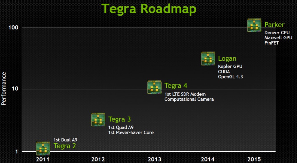
As soon as it turned out that TSMC’s 16nm FinFET fabrication process would not be ready for mass production in the first half of 2015, Nvidia decided to incorporate “Denver” into the 64-bit version of Tegra K1 “Logan” (with “Kepler” graphics), which is made using 28nm fabrication process. The “Parker” chip was thrown out from Nvidia’s roadmap and the code-named “Erista” SoC replaced it.
Tegra roadmap, image by AnandTech
The “Denver” core was developed from the ground-up for the 16nm FinFET process technology. Integrating the core into a 28nm design was hardly an optimal choice given die size, power consumption and other factors. Nvidia has never explained why it needed to create 64-bit Tegra K1 chip based on the “Denver” cores. Most probably, it needed software developers to lay their hands on its custom microprocessor design in order to ensure that future apps will be fully optimized for Nvidia’s high-performance ARMv8 cores.
It is logical to expect Nvidia to incorporate “Denver” into its application processors to be made using 16nm FinFET process technology, just like it planned originally with the code-named “Parker” AP. Unfortunately, since TSMC’s 16nm FinFET manufacturing technology is at least two quarters away, it is unknown when Nvidia will be able to commercialize such chip. Depending on design readiness, this could happen only late this year at the earliest. Keeping in mind Nvidia’s typical Tegra schedules, expect the new chip to arrive only in early 2016.
Discuss on our Facebook page, HERE.
KitGuru Says: It looks that the mess TSMC and other foundries created with availability of process technologies also generated a mess with product designs. As a result, Nvidia had to redesign its “Maxwell” graphics architecture as well as to change its Tegra roadmap significantly.