

We have already mentioned the 5960X's eight physical cores so let's run through some of its other performance characteristics.
Firstly there's the 3.0GHz base clock for all cores. Turbo Boost 2.0 increases this operating speed to 3.5GHz when a fraction of the total core count is active, although modern motherboards typically use profiles that glue every core at its maximum multiplier 100% of the time. And when 3.5GHz simply isn't enough, users can leverage the fully unlocked core ratio multiplier to further increase the CPU frequency.
Support for DDR4 extends to a frequency of 2133MHz natively. As has been the case for recent Intel processors, the maximum memory frequency supported with the right motherboard extends past the chip's default value.
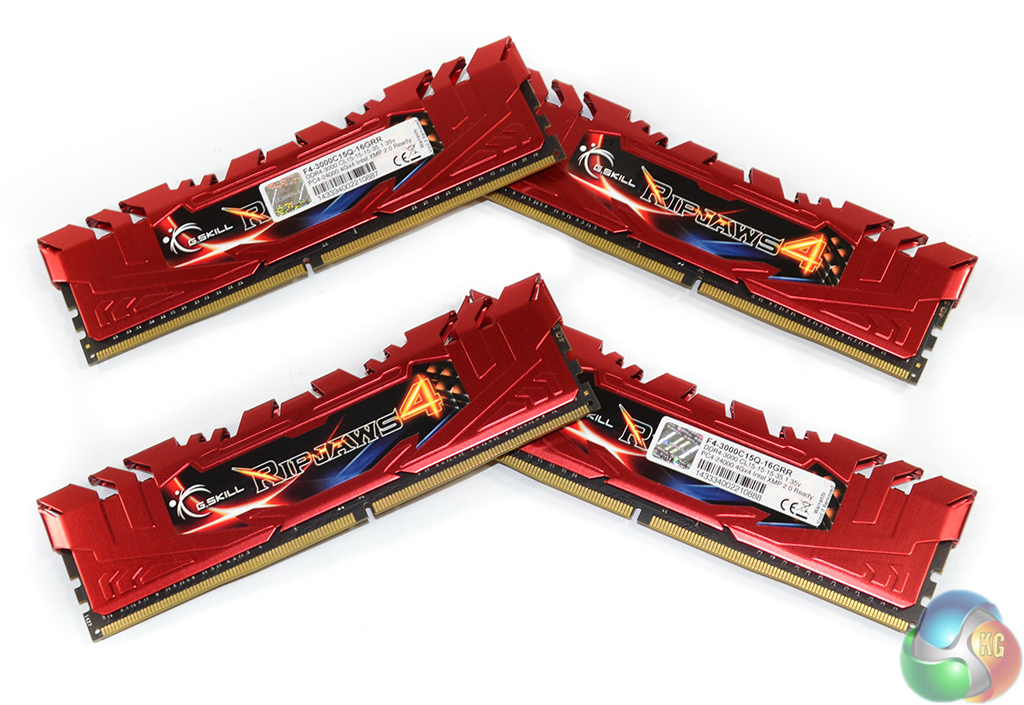
We had no problem booting up with G.Skill's 3000MHz Ripjaws4 memory kit on the Asus X99 Deluxe, although we do know that other motherboard vendors have been experiencing problems reaching stability at a 3GHz DRAM frequency.
Past 2666MHz and the CPU shifts up to a BCLK of 125MHz (using the 1.25X clock multiplier). This is different to past Intel chips; the 4770K/4790K can run memory speeds all of the way up to 2933MHz off a 100MHz base clock (when using the 100:133 BCLK:DRAM ratio and a 22x memory multiplier). A 125MHz BCLK is not an issue, it just adjusts the frequencies available to the CPU.
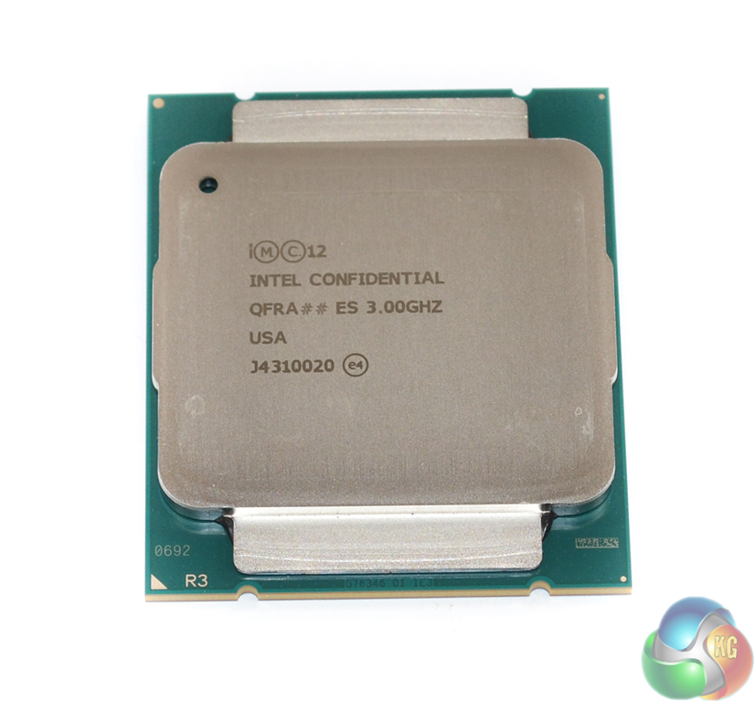
(Haswell-E Core i7 5960X left. Ivy Bridge-E Core i7 4960X right.)
Heatspreader design is something that has changed for Haswell-E. Previous HEDT processors used a block of metal that engulfed the vast majority of the chip. Haswell-E shrinks the heatspreader area by a marginal amount and also tweaks its design.
At a recent press event we asked Intel what material was used beneath the heatspreader. While we didn't get a firm answer, it was suggested that the chip uses solder in a similar way to previous HEDT parts. And that's a good sign when the chip's TDP is a lofty 140W.
As a note, this is the first Intel chip that I recall handling personally to be manufactured in the USA.
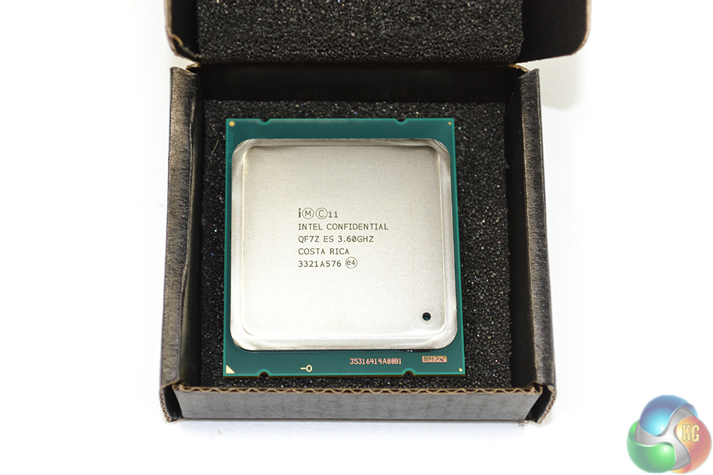
(Haswell-E Core i7 5960X left. Ivy Bridge-E Core i7 4960X right.)
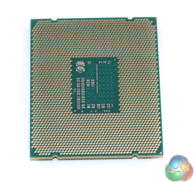
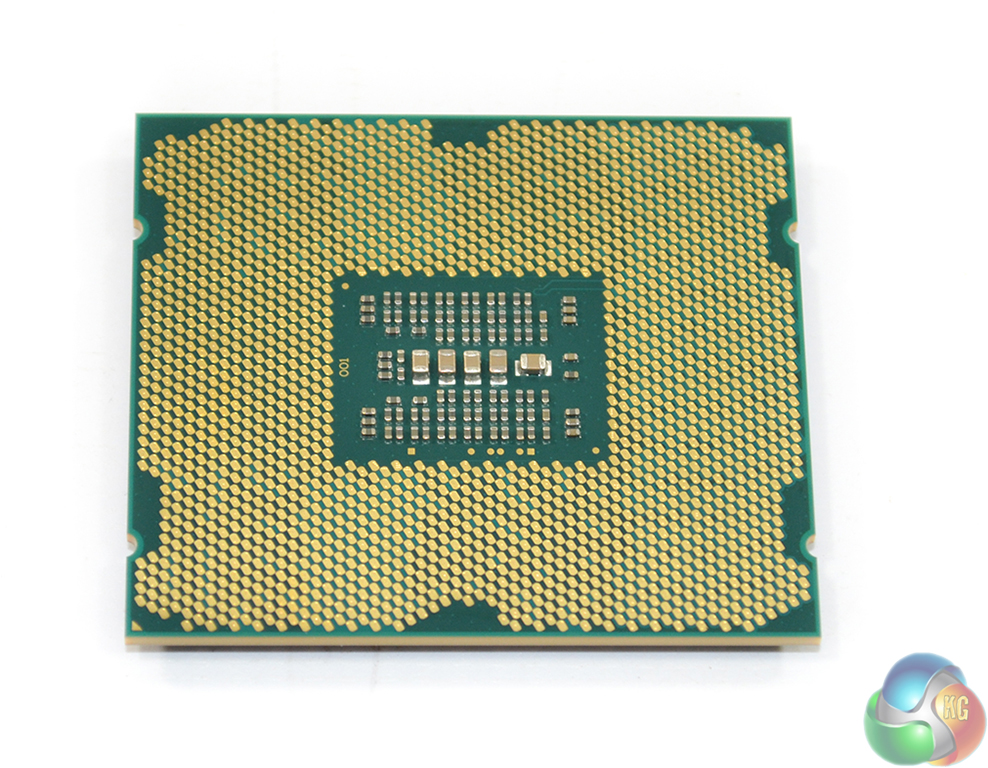
Layout of the underside components also shows notable differences between the two processors. HSW-E loses a few of the capacitors found on IVB-E, although it does increase pin count.
Asus makes use of the additional pins with a patent-pending technology it calls Asus OC Socket. The motherboard socket features contact points for the additional pins to allow increased current/voltage delivery.
Haswell-E chips ARE NOT compatible with LGA 2011 (X79) motherboards, and vice versa. The main reason for this incompatibility is HSW-E's support for DDR4 memory. Intel would have given itself and consumers headaches by providing capacity for both LGA 2011 and LGA 2011-v3 chips on a single motherboard. A new socket was deemed the favourable approach.
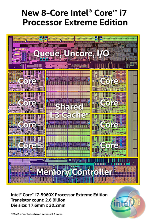
2.6 billion 22nm transistors on a 355.5mm2 die – now that's advanced manufacturing.
Each of the eight physical cores eats into the processor's 20MB quota of level 3 cache. A notable difference between the HEDT HSW-E parts and a mainstream Haswell-based chip, such as the 4770K, is the on-board GPU's exclusion. This frees up valuable die space for more cores and cache.
Haswell-E's key partner in the HEDT platform is the X99 chipset. We are going to brush over the chipset and its features for this article as they will be explored in more detail in our upcoming barrage of motherboard reviews.
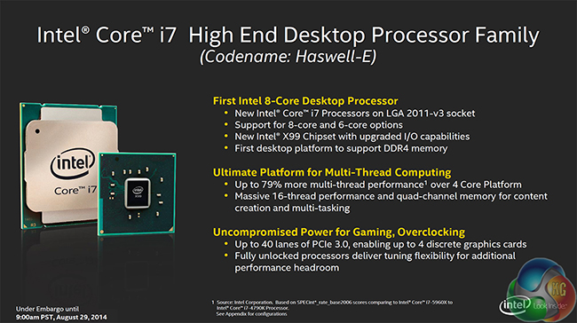
Referencing gaming performance though, the Haswell-E 5960X and 5930K both provide 40 PCIe 3.0 lanes. Intel reduces the 5820K's lane count to 28. Although the above slide suggests that up to four graphics cards can share the lanes, the real number is actually five. Splitting the lanes between five GPUs results in x8 PCIe 3.0 links for each. That's particularly useful for workstation users.
From a gaming perspective, there is plenty of bandwidth to support multi-VGA configurations, hence many of the lane count headaches caused by the mainstream platform are avoided. We asked Intel if the lanes can be split down to x4 and then used for storage links, but they informed us that doing so necessitates an additional controller.