

Although Advanced Micro Devices said earlier this year that it would use 20nm process technology from Taiwan Semiconductor Manufacturing Co. for its future chips, it looks like the company readies two new graphics processing units (GPUs) that will be made using TSMC’s 28nm HPM [high-performance mobile] process technology.
Synapse Design, an industry leader in semiconductor design services that helps AMD and multiple other companies to develop their chips, recently said that it had taped out (the point at which its customer sends photomask of a chip to the manufacturer) two graphics processors that will be manufactured using 28nm HPM process technology at TSMC. Since AMD is the only GPU designer among Synapse Design’s clients, it is logical to assume that the GPUs were designed by the Sunnyvale, California-based chip designer.
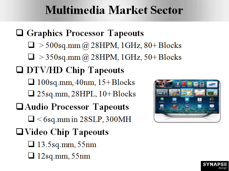
One of the GPUs is claimed to be very large – over 500 square millimeters – another is claimed to have 350sq.mm die size. For comparison, AMD’s current flagship Hawaii GPU features 438sq.mm die size, whereas the previous-gen top-of-the-range graphics processor – Tahiti – was 352sq.mm in size.
The slide from Synapse Design most likely covers the company’s press release from the 25th of June, 2014, which reveals tape-outs in the first half of the year. The slide was located at AnandTech forums.
The fact that AMD taped out at least two new GPUs in the first half of the year (it is likely that the company taped out three new GPUs: Maui, Iceland and Tonga) means that the chip designer can officially introduce them in the late Q3 or the early Q4.
Earlier it was reported that AMD’s new graphics processors due out this year are based on a fresh incarnation of the GCN [graphics core next] architecture, which could be called the “new GCN” (some call it GCN 1.2 or even GCN 2.0). Previously it was rumoured that the new GCN would support a number of enhancements related to heterogeneous system architecture (HSA), including GPU compute context switch as well as GPU graphics pre-emption, something that is already supported by the Kaveri accelerated processing unit. In addition, it is likely that the new graphics processors will fully support existing technologies, such as DirectX 11.2, Eyefinity, TrueAudio and so on.
Since the new flagship GPU from AMD will be larger than the current-generation Hawaii chip, expect it to feature higher amount of stream processors, texture units and raster operating units in addition to other improvements. Thanks to the fact that the new 28nm HPM fabrication process will enable considerably higher clock-rates, the 350sq.mm chip will likely run at rather extreme frequencies to deliver performance comparable or higher to that of the code-named Tahiti.
AMD did not comment on the news-story.
Discuss on our Facebook page, HERE.
KitGuru Says: It looks like we have finally got the first semi-official confirmation that AMD readies at least two new graphics processing units for 2014. Meanwhile, the future plans of the company are not completely clear. Given the fact that this year AMD is going to refresh its product line-up using 28nm GPUs, it remains to be seen whether the company will actually use 20nm process technology developed by TSMC. The latter’s 16nm fabrication tech is near and AMD will likely have enough time to design chips for the new node.