

The high-bandwidth memory (HBM) introduced along with AMD’s code-named “Fiji” graphics processing unit radically changes the way graphics adapters are built and also dramatically improves potential performance of future graphics processing units. But while HBM looks ingeniously simple on paper, it was extremely hard to develop and is not easy to build. In fact, AMD started to work on what is now known as HBM as early as in 2006 – 2007.
The need for speed
Memory bandwidth has been a performance-limiting factor for graphics processors since the introduction of the first gaming-grade graphics cards, three-dimensional games and 32-bit colour back in the nineties. In a bid to considerably increase performance of a graphics adapters, IHVs [independent hardware vendors] had to bolster bandwidth of their DRAM [dynamic random access memory], which was not always easy.
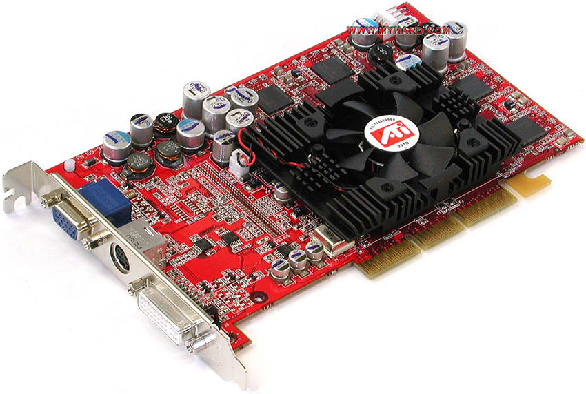
There are several ways to increase memory bandwidth on a graphics card: to rise memory clock-rate, to widen memory interface, or to use a more efficient memory technology. After increasing frequencies of graphics DRAM to rather high levels in 1997 – 1998, Nvidia Corp. was the first company to start using the double data rate (DDR) memory (which transfers data on both the rising and falling edges of the clock signal, the technology known as double-pumping) on its GeForce 256 DDR graphics cards in 1999 and doubled bandwidth available to the GPU. ATI Technologies introduced the world’s first graphics card with 256-bit memory bus in 2002 and doubled memory bandwidth of graphics processors once again. In 2002 – 2003 new memory technologies – GDDR2 and GDDR3 – designed specifically for GPUs and supporting quad-pumping were introduced and doubled available bandwidth another time.
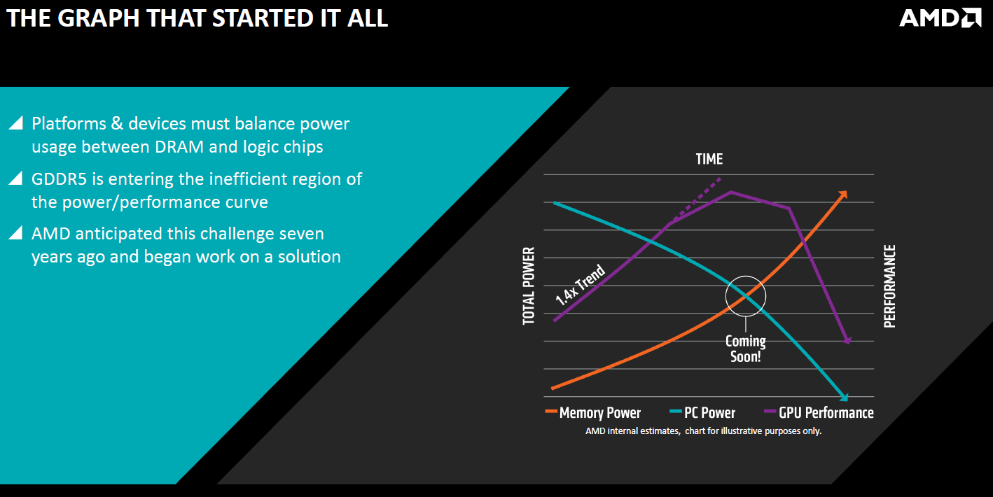
But memory bandwidth improvements in the early 2000s did not come for free. Increases of clock-rates and data rates amplified power consumption of memory chips. Wider memory interfaces required more memory ICs, which also increased power requirements of add-in-boards.
By 2006 – 2007, when the work on the ATI R600 graphics processor with 512-bit memory bus as well as on the GDDR4 and the GDDR5 memory technologies was essentially completed, it became clear that memory consumed a lot of power already and would consume even more over time. Since ATI and Nvidia planned to use their GPUs for high-performance computing (HPC) applications, which require a lot of local memory, it was obvious that power consumption of GDDR was going to become a problem.
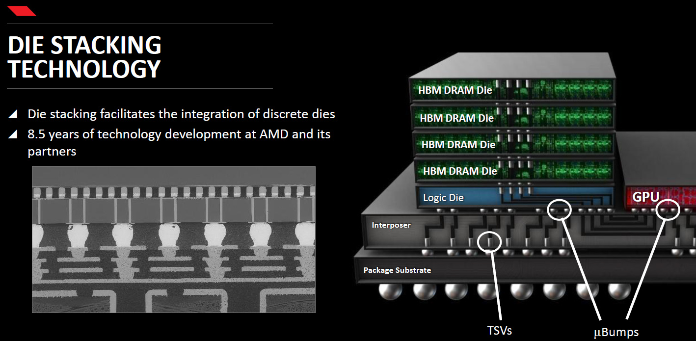
At the time, new memory tech development team at ATI Technologies led by Joe Macri came up with an idea of brand-new memory technology, which could provide extreme bandwidth while consuming a low amount of energy. The key elements of the new technology were multi-layer memory devices with an ultra-wide interfaces that used silicon interposer to connect to a processing device.
Brief history of HBM
Modern technologies take a long time to develop. For example, the work on DDR4 started back in 2005, a couple of years before DDR3 was commercially launched. Similarly, ATI Technologies (which AMD acquired in 2006) started to think about high-bandwidth memory with low power consumption about a decade ago, before the company helped to commercialize GDDR4 in 2006 and GDDR5 in 2008. The work on what is now known as HBM began sometimes in 2006 – 2007 and in 2013 the technology became an industry standard.
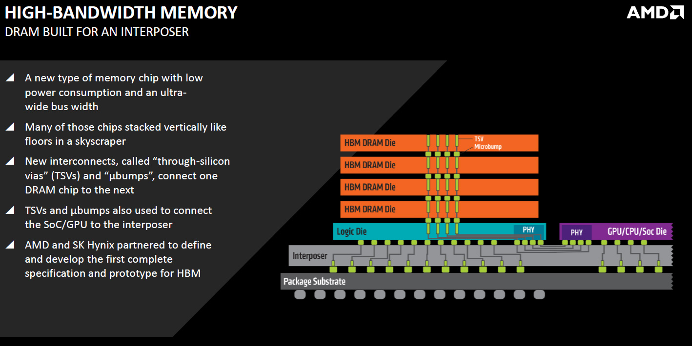
Architecturally, the first-generation high-bandwidth memory (JESD235) uses a protocol similar to that of the original DDR, which development kicked off in 1996 and was concluded in mid-2000. But a in a bid to finish the new standard, AMD, SK Hynix and other developers had to create a massive amount of additional technologies that ultimately facilitated creation of graphics processors like AMD’s “Fiji”.
There are several key technologies that empower HBM:
- Memory chips with multiple vertically stacked memory devices interconnected using through-silicon-vias (TSVs) and microbumps and then placed on a base logic die.
- Silicon interposer that connects memory ICs to host processor using an ultra-wide interface. Silicon interposer is made using a photolithography technology in a semiconductor fabrication plant.
- Host processor with ultra-wide memory interface.
Development of new technologies requires a lot of prototyping activities in general. Before AMD and SK Hynix proceeded to standardize their HBM memory with JEDEC in 2010, the companies had to design multiple implementations of their new technologies and learn how they operated in real-life.
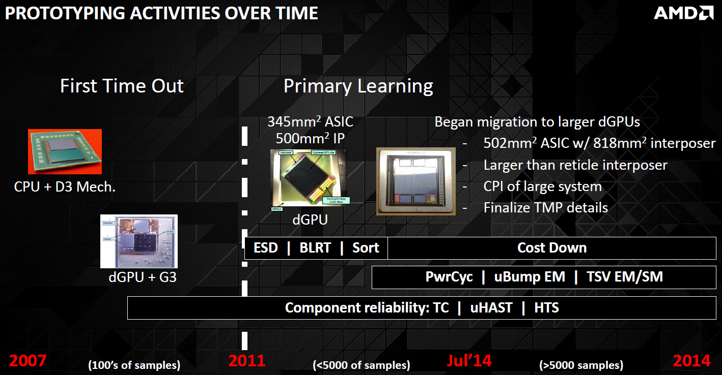
AMD started to experiment with interposers and processors back in 2007. The first GPU to connect to memory using an interposer was the RV635, which powered ATI Radeon HD 3650/3670 graphics adapters. Eventually, AMD experimented with interposers and the “Cypress”, which was the world’s first DirectX 11-supporting graphics processor. Both the RV635 and the “Cypress” were based on the TeraScale architecture (gen 1 and gen 2), which was succeeded by the GCN [graphics core next] architecture in 2012.
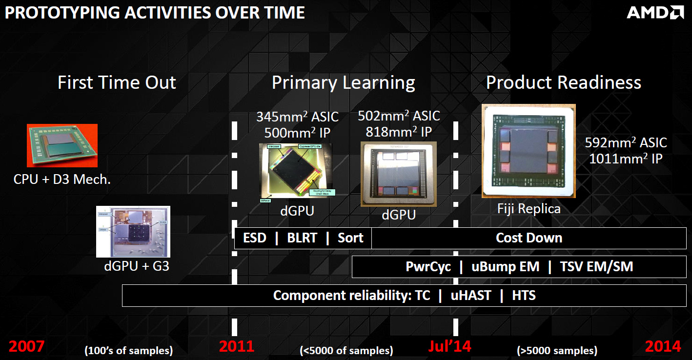
The JESD235 standard was published in October, 2013, when the work on AMD’s “Fiji” was well underway and the graphics processing unit was months away from tape-out.
The HBM saga continues
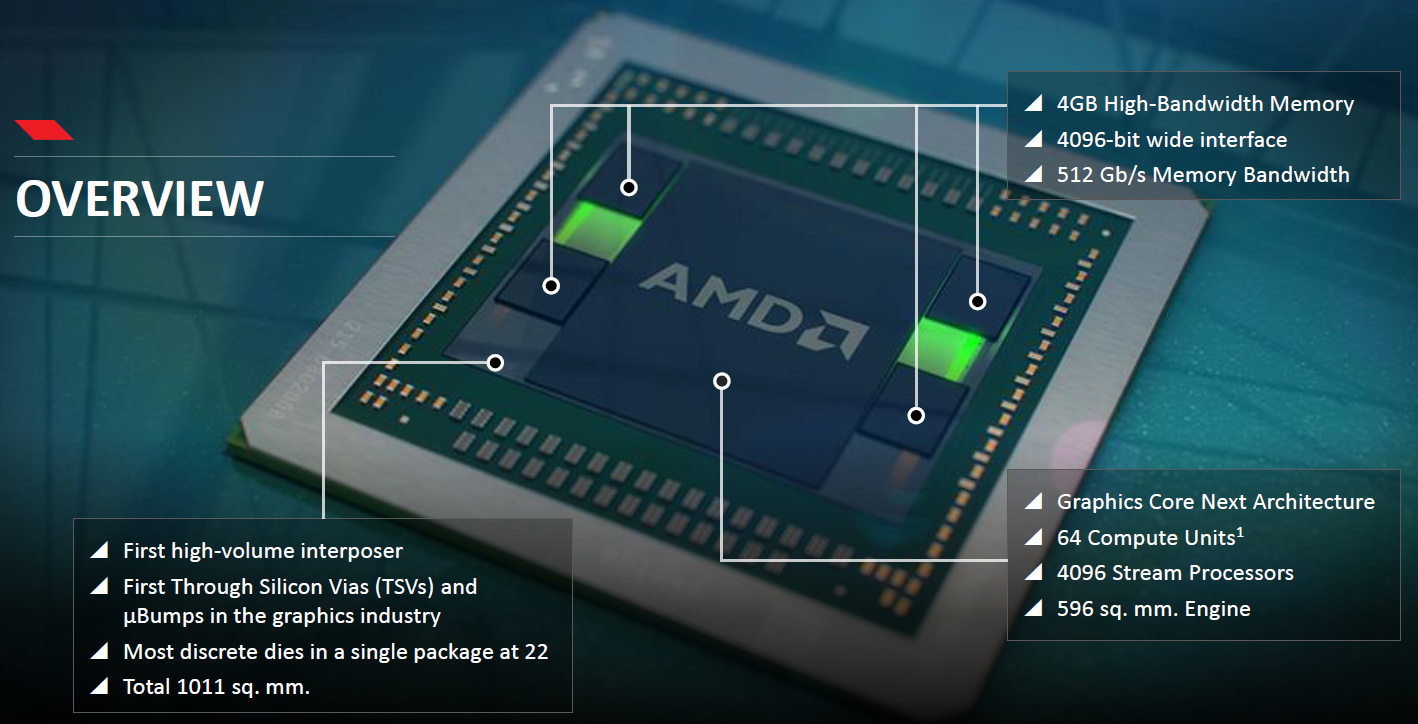
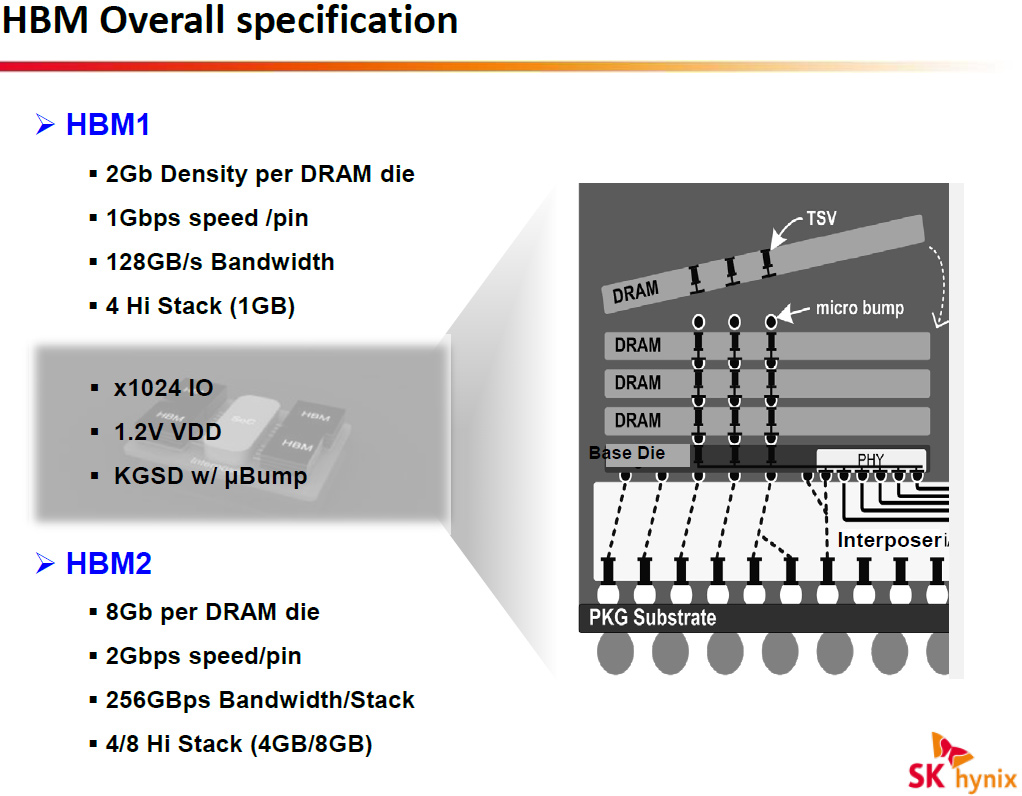
The first-generation HBM (HBM1) stacks four DRAM dies with two independent 128-bit channels per die on a base logic die, creating a memory device with a 1024-bit interface. Each channel supports 1Gb capacities (2Gb per die), features 8 banks and can operate at 1Gb/s data-rate (1GHz effective DDR clock-rate). As a result, each HBM 4Hi stack (4 high stack) package can provide 1GB capacity and 128GB/s memory bandwidth. AMD’s Radeon R9 Fury X flagship graphics adapter features 4GB of HBM memory with unprecedented bandwidth of 512GB/s. While the first-gen HBM has limitations when it comes to capacity, it allows to create very small and very high performance graphics solutions thanks to the fact that HBM chips are smaller than GDDR5 ICs.
The second-generation HBM (HBM2) utilizes 8Gb dies with two 128-bit channels featuring 16 banks and sporting up to 2Gb/s data-rates (2GHz effective DDR frequency). The architecture of the HBM2 will let manufacturers built not only 4Hi stack (4 high stack) packages, but also 2Hi stack and 8Hi stack devices. As a result, memory producers will be able to assemble HBM2 memory chips with up to 8GB capacity (8Hi stack) and up to 256GB/s bandwidth (2Gb/s data rate, 1024-bit bus).

Architectural advantages of HBM2 will allow GPU developers to use it not only for ultra-high-end applications with 4096-bit memory bus, but also for adapters that do not require extreme performance. Next-generation enthusiast-class graphics cards based on AMD’s “Greenland” graphics processors as well as Nvidia’s GP100 (“Pascal”) GPUs will feature 8GB – 16GB of HBM memory with up to 1TB/s bandwidth. Samsung Electronics forecasts that over time HBM will enable add-in-boards with up to 48GB of memory.
The third-generation HBM is in development and engineers currently do not share any information about it. It is logical to expect further increases of capacities as well as performance. While we have no idea how additional capacities and performance will be achieved, we are pretty sure that engineers at companies like AMD are already playing not only with prototypes of future implementations of HBM, but also with something that will succeed them a long time down the road.
Discuss on our Facebook page, HERE.
KitGuru Says: The evolution of GDDR memory slowed down in 2007 (partly because Joe Macri and the team went on to develop HBM) and HBM promises to bring back rapid increase of memory bandwidth in the coming years. How far will HBM go? Will we see graphics cards with 2TB/s or 4TB/s memory sub-systems in the next five to seven years? We do not know for sure, but it looks like exciting times are coming back!