
Although Intel Corp. does not plan to use lithography with extreme ultraviolet (EUV) wavelength with its 10nm fabrication process, it looks like other makers of semiconductors still pin hopes to take advantage of the EUV in connection with 10nm technology.
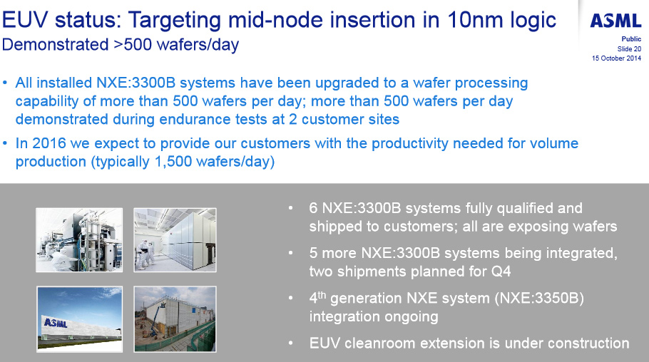
ASML, one of the leading producers of semiconductor manufacturing tools, on Wednesday made an update regarding progress of its EUV [extreme ultraviolet] lithography equipment. The company indicated that it has upgraded its NXE:3300B systems at customers’ sites to manufacture more wafers per hour than it was previously possible. It also revealed that it is on-track to ship NXE:3350B systems suitable for commercial production of chips using extreme ultraviolet lithography in 2016. Moreover, there is at least one customer interested in using it with 10nm fabrication process.
So far ASML shipped six NXE:3300B EUV test systems to customers. Previously the tools were only capable of processing 200 300mm wafers per 24 hours. Thanks to upgrade of the EUV light source inside the test systems, they are now capable of processing 500 wafers per 24 hours. Meanwhile, for high-volume manufacturing wafer scanners should process 1500+ wafers per 24 hours.
“Our EUV program showed substantial progress in the quarter,” said Peter Wennink, president and chief executive officer of ASML. “All installed NXE:3300B systems have been upgraded to a wafer processing capability of more than 500 wafers per day. Two customers conducted endurance tests that demonstrated this capability of more than 500 wafers in a 24-hour period. We continue executing programs that should consistently deliver this level of performance, which our customers require by the end of the year.”
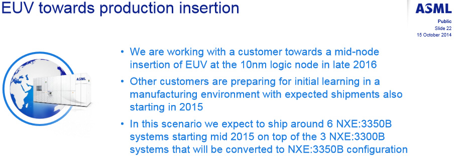
Previously it was expected that the semiconductor industry (i.e., leading makers of chips like Intel) would use EUV lithography starting from 2015 and 10nm process technology. However, delays at ASML postponed adoption of EUV lithography and, for example, Intel has no plans to use the tech for 10nm production. Still, ASML claims that there is an unknown customer planning to start using EUV in late 2016 with 10nm process technology.
“We are working with a customer towards a mid-node insertion of EUV at the 10nm logic node expected in late 2016,” said Mr. Wennink. “Other customers are preparing for initial learning in a manufacturing environment. In this scenario we expect to ship around six NXE:3350B systems starting mid-2015, on top of the three NXE:3300B systems that will be converted to NXE:3350B configuration.”
Discuss on our Facebook page, HERE.
KitGuru Says: It is not completely clear what the “mid-node insertion” is. By late 2016 only Intel and TSMC are expected to have more or less ready 10nm process technology. Both companies require extremely high volumes and will hardly bother with two types of 10nm fabrication processes: one with EUV, another without EUV. Still, TSMC has confirmed interest to use EUV with 10nm fabrication process for a number of times…