

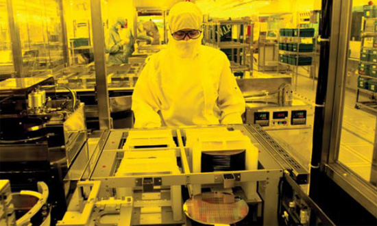
GlobalFoundries and Samsung Semiconductor, two leading contract makers of chips, on Thursday signed a pact under which they will be able to jointly produce chips using 14nm FinFET fabrication process. The two foundries will “synchronise” not only their general jointly-developed process technologies, but peculiarities of their manufacturing processes that are implemented on fabs. This will allow the two firms to jointly fulfil large-scale 14nm orders.
GlobalFoundries and Samsung Electronics are considerably behind their arch-rival Taiwan Semiconductor Manufacturing Co. in terms of production capacities. As a result, TSMC manages to get lucrative large-scale orders from leading companies to produce their chips since it can guarantee that all the batches of products will feature the same characteristics and quality. TSMC is a key partner of AMD, Nvidia, Qualcomm and other developers that require vast amounts of chips.
GlobalFoundries and Samsung already co-develop process technologies together being parts of Common Platform Technology Alliance, so their fabrication processes are very similar. Going forward, the two companies plan to synchronize actual production facilities and will use a coordinated copy-smart approach involving materials, process recipes, integration and tools. The companies will also run fab-sync test chips on a regular basis to ensure that the fabs making chips using 14nm FinFET process are exactly the same. As a result, GlobalFoundries and Samsung will give their customers the ability to produce a single GDS II design at multiple manufacturing facilities. The two foundries hope that this will help them to land orders from large customers, such as Apple.
The new collaboration will involve synchronization of production lines at leading-edge semiconductor manufacturing capabilities, including Samsung’s fabs in Hwaseong, Korea and Austin, Texas, as well as GlobalFoundries’ fab in Saratoga, New York.
GF’s and Samsung’s 14nm process technology is based on a modular architecture that uses 14nm FinFET devices combined with 20nm-LPM process back-end-of-line (BEOL) interconnect flow. This allows chip designers cut-down power consumption, improve performance of new chips, but not to substantially shrink their sizes or costs.
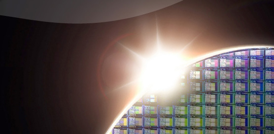
Mass production for the 14nm FinFET technology will begin at the end of 2014.
“This unprecedented collaboration will result in a global capacity footprint for 14nm FinFET technology that provides AMD with enhanced capabilities to bring our innovative IP into silicon on leading-edge technologies,” said Lisa Su, senior vice president and general manager of global business units at AMD. “The work that GlobalFoundries and Samsung are doing together will help AMD deliver our next generation of ground-breaking products with new levels of processing and graphics capabilities to devices ranging from low-power mobile devices, to next-generation dense servers to high-performance embedded solutions.”
Discuss on our Facebook page, HERE.
KitGuru Says: This is not the first time when Samsung and GlobalFoundries synchronise their manufacturing technologies and offer collaborative manufacturing. It looks like the foundries this time actually did numerous steps towards complete synchronisation, but it is unlikely that everything will be 100 per cent similar simply because different fabs use various manufacturing equipment. Still, in case GF and Samsung manage to land more orders from customers thanks to their collaboration, then this is a good news for the two.