
Nvidia Corp. has reportedly taped out its next-generation high-performance graphics processing unit that belongs to the “Pascal” family, according to a market rumour. If the information is correct, then Nvidia is on-track to release its new GPU around mid-2016. The company needs its “Big Pascal” graphics processor to build next-generation Tesla accelerators for high-performance computing applications and better compete against AMD on the market of consumer GPUs.
An anonymous person presumably with access to confidential information in the semiconductor industry revealed in a post over at Beyond3D forums that Nvidia had already taped out its next-generation code-named GP100 graphics processing unit. Nowadays, a tape-out means that the design of an integrated circuit has been finalized, but the first actual chips materialize only months after their tape-out.
Tape-out is the final stage of the design cycle of an integrated circuit, the point at which the artwork of the IC is sent to a maker of photomasks. Once the set of photolithographic masks is ready and verified, it is sent to a contract manufacturer of the chip, which produces the first working samples of the IC. Today’s mask sets contain 50 – 70 (up to 100) photomasks and it takes 15 – 20 hours to write a typical mask. It may take several weeks to prepare a mask-set. Production cycle of a complex FinFET processor is around 90 days from wafer start to chip delivery. As a result, it takes several months to prepare a set of photomasks and build an actual chip nowadays. Hence, if Nvidia taped-out of the GP100 in May, then the company will get the first samples of its GP100 in August. Nowadays high-volume production of chips starts between nine and twelve months after the initial tape-out.
The world’s No. 1 producer of discrete graphics processors will reportedly use one of Taiwan Semiconductor Manufacturing Co.’s 16nm FinFET fabrication technology to make its “Big Pascal” GPU. Given the timeframe of the tape-out, it is highly likely that Nvidia uses TSMC’s advanced 16nm FinFET+ (CLN16FF+) manufacturing technology. According to the post, the BP100 is Nvidia’s first 16nm FinFET chip and the company has changed its approach to roll-out of new architectures. Instead of starting from simple GPUs and introducing biggest processors quarters after the initial chips, Nvidia will begin to roll-out “Pascal” with the largest chip in the family.
Nvidia’s “Pascal” architecture represents a big leap for the company. Thanks to all-new architecture, the Nvidia's next-gen GPUs will support many new features introduced by DirectX 12+, Vulkan and OpenCL application programming interfaces. The 16nm FinFET process technology will let Nvidia engineers to integrate considerably more stream processors and other execution units compared to today’s GPUs, significantly increasing overall performance. In addition, next-generation graphics processing units from Nvidia will support second-generation stacked high-bandwidth memory (HBM2). The HBM2 will let Nvidia and its partners build graphics boards with 16GB – 32GB of onboard memory and 820GB/s – 1TB/s of bandwidth. For high-performance computing (HPC) applications, the “Big Pascal” chip will integrate NVLink interconnection tech with 80GB/s or higher bandwidth, which will significantly increase performance of “Pascal”-based Tesla accelerators in supercomputers. Moreover, NVLink could bring major improvements to multi-GPU technologies thanks to massive bandwidth for inter-GPU communications. According to Nvidia's estimates, graphics adapters based on “Pascal” architecture should deliver two to ten times higher performance than comparable graphics processors today in peak scenarios.
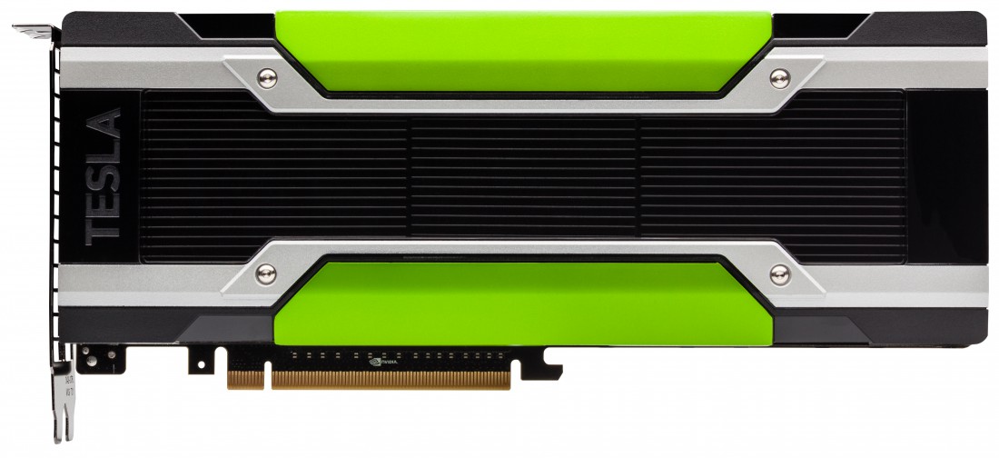
Nvidia needs GP100 chip in order to build next-generation Tesla accelerators for supercomputers. Since “Maxwell” architecture (even the GM200) lacks native support for double precision (DP) FP64 computing, it cannot be used for Tesla cards. As a result, Nvidia currently offers Tesla accelerators featuring GK110 and GK210 chips, which are basically three years old. The release of the “Big Pascal” will help Nvidia to boost sales of Tesla cards for HPC applications.
The accuracy of predictions of the Beyond3D forum member could not be verified, but some of his previous posts indicate that he has access to information that is not yet public. The post in the forum on Friday was republished by 3DCenter, a web-site known for predictions in the field of graphics processing units.
Nvidia did not comment on the news-story.
Discuss on our Facebook page, HERE.
KitGuru Says: On the one hand, the rumour comes from one source without a track record and should be taken with a huge grain of salt. On the other hand, Nvidia needs “Big Pascal” to update Tesla accelerators as soon as possible. If Nvidia wants to release its GP100-based products in mid-2016, then the chip has been taped-out by now.