

Samsung Foundry this week said that it had officially added its 10nm FinFET fabrication technology into its foundry roadmap. The company also clarified that it will start mass production of chips using its third-generation manufacturing process with FinFET transistors in late 2016, which means that the first 16nm commercial chips from Samsung will hit the market in 2017.
“We have a full PDK [process development kit] and silicon-verified IP available, and are, currently, running MPWs [multi-project wafer] now for our lead customers,” said Kelvin Low, senior director of marketing at Samsung Foundry. “With mass production scheduled from late 2016 we are excited about this next phase of our foundry business. Early designs activities have already sparked some interesting discussions.”
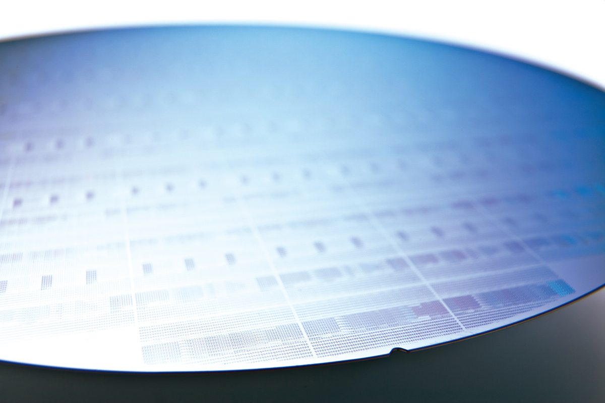
Samsung’s 10nm fabrication process is an all-new technology that features its own back-end-of-line interconnect flow in addition to all new front-end-of-line features, providing performance, power and area scaling. It is expected that Samsung’s 10nm FinFET sports considerably smaller transistor fin, transistor gate and interconnect pitches compared to the company’s 14nm process technologies. Shrinking geometry of all pitches results in higher performance, increased transistor density and lower per-transistor costs, something that will be a huge benefit for many companies who use Samsung Foundry’s services.
Earlier this year Samsung already demonstrated a 300mm wafer processed using its 10nm technology. By now the company has finalized the vast majority of specifications of the process as well as process development kits.
Samsung expects to start trial production using 10nm FinFET manufacturing technology in late 2015. The company will be able to start volume production using the process tech in late 2016.
[yframe url='http://www.youtube.com/watch?v=6XtBphQvFFg']Previously it was expected that Samsung would use its 10nm fabrication technology to produce its next-generation Exynos application processor for Samsung Galaxy S7 smartphones. While the company may try to do this, it is more likely that the next-gen system-on-chip for the flagship handset will be produced using the second-generation 14nm FinFET (14nm low-power plus, 14LPP) process.
Discuss on our Facebook page, HERE.
KitGuru Says: Looks like the race for 10nm has officially begun. TSMC and Samsung are ahead of GlobalFoundries and UMC, which is not really surprising as the two companies are competing for one customer, Apple. But the real question is whose manufacturing process will be better and who will be able to produce more leading-edge chips.