
Samsung Electronics plans to concentrate on expansion of production capacities used to make its 3D V-NAND memory going forward. A media report claims that the South Korean conglomerate no longer plans to build new manufacturing facilities for production of traditional planar NAND flash.
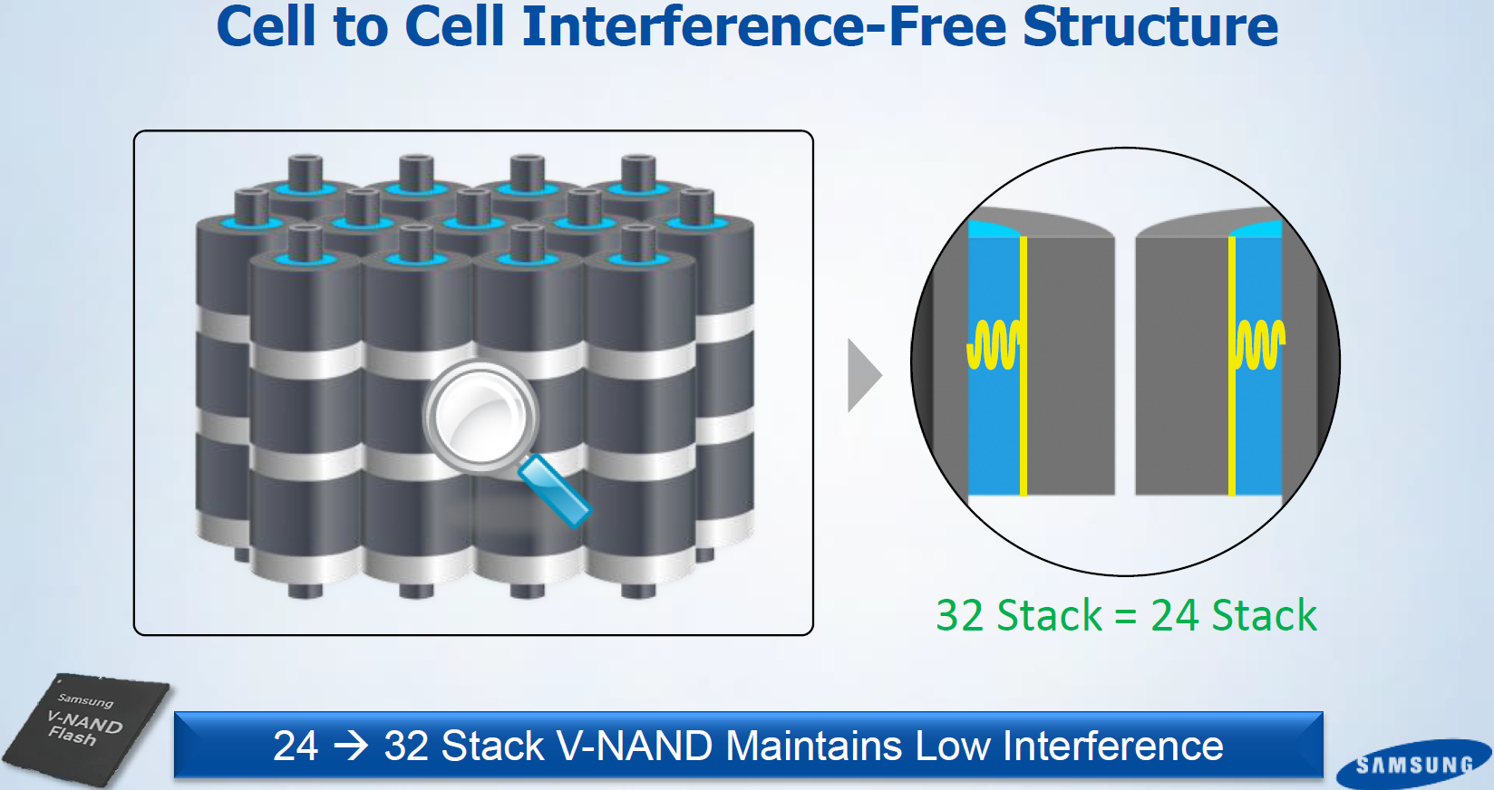
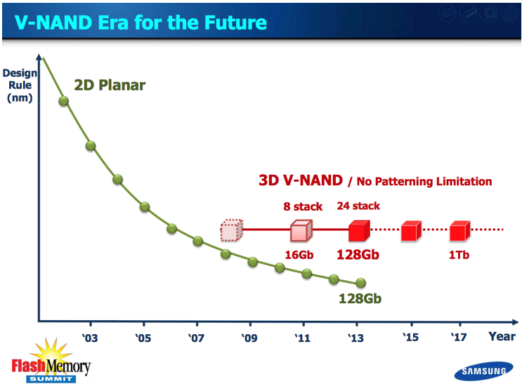
NAND flash was invented by Toshiba Corp. in 1984 and while its architecture has been rapidly evolving over the years, its planar structure remained largely unchanged. In the recent years Samsung Electronics introduced vertical NAND, which, while using the same principles as planar NAND, provides a number of benefits. The vertical layers connected using the through-silicon-vias (TSVs) of the 3D V-NAND allow larger areal bit densities without requiring smaller individual cells (hence, eliminating need for ultra-thin manufacturing technologies), which means higher write/erase endurance, general reliability and performance.
Samsung claims that its 3D V-NAND exhibits at least two times the endurance and writes data (tPROG, program time) at least twice as fast as multi-level-cell (MLC) type planar NAND flash memory made using one of the latest manufacturing processes. Besides, 3D V-NAND is also more energy-efficient than planar NAND memory: it consumes around 40 per cent less of power.
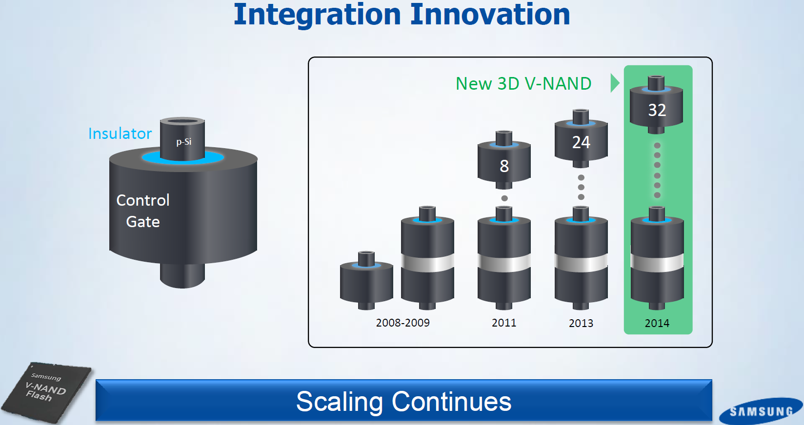
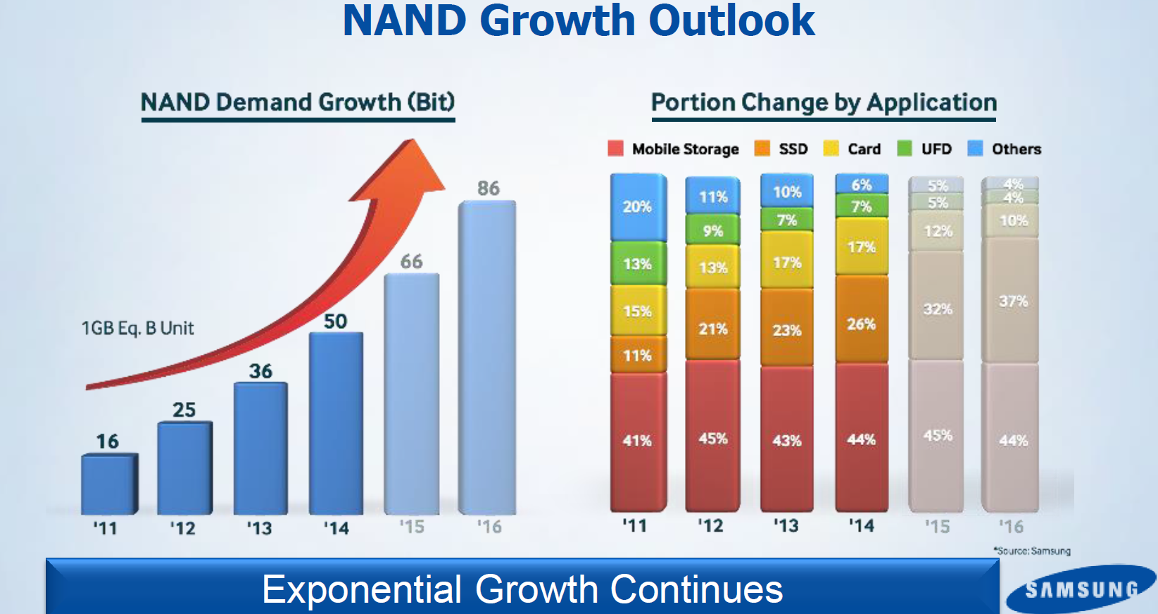
Perhaps, what is even more important, 3D NAND allows to rapidly increase capacities of NAND flash chips and solid-state drives, something the industry needs badly. According to predictions by Samsung, total available market for NAND flash memory will grow to 66 billion 1GB equivalent memory chips this year, up from 50 billion of 1GB equivalent memory devices. As a result, it is getting crucial to increase density of NAND flash memory ICs [integrated circuits], something, which 3D NAND technology allows to do relatively easily.
Samsung’s 3D V-NAND has become mature enough in the recent years and now the company plans to significantly increase production of this type of non-volatile computer storage medium. In fact, BusinessKorea reports that Samsung no longer plans to build new facilities to make planar NAND flash, but to focus solely on expansion of 3D V-NAND.
“Samsung Electronics will not set up a general NAND flash plant any longer, but concentrate on V-NAND from now on,” a source with knowledge of Samsung’s plans is reported to have said.
At present Samsung produces 3D V-NAND memory at one its facilities in Hwaseong, South Korea, as a well as at a dedicated 3D NAND fab in Xi’an, China. The Chinese factory can process around 100 thousand 300mm wafers per month. Eventually the company plans to expand its Xi’an manufacturing complex in a bid to produce 300 thousand 300mm wafers per month, the report claims. Manufacturing capacities used to make 3D NAND memory may not need leading-edge process technologies, but they require specific advanced equipment.
Planar NAND flash memory will continue to be produced and utilized for various applications for many years to come. Even Samsung Electronics itself will likely introduce one or two more manufacturing technologies for making NAND. Moreover, the company will likely upgrade at least some of its current fabs that make planar flash memory to new fabrication processes.
Samsung’s decision to concentrate 3D V-NAND capacities clearly indicates where the market is going. In fact, Samsung is not alone with its focus on 3D NAND. Other makers of flash, including Toshiba/SanDisk, SK Hynix and Micron are also about to start making 3D NAND for the same reasons as Samsung. Moreover, Micron Technology, which began to expand its fab 10N in Singapore in early March, also intends to use its new manufacturing capacities to make second-gen 3D NAND flash memory.
Samsung did not comment on the news-story.
Discuss on our Facebook page, HERE.
KitGuru Says: Given all the advantages that 3D NAND has over planar NAND, it makes a great sense for makers of flash memory to focus on the former instead of the latter. One of the things that needs to be mentioned is that new production facilities are getting more and more expensive. In fact, some analysts believe that 3D NAND technology is more than two times more capital intensive than planar NAND. Therefore, in the long term, those, who want to stay in the business, have to be big and profitable. With $56 billion in its wallet, Samsung can be rather confident about its future.