

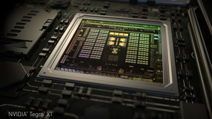
Nvidia Corp. on Monday introduced its latest addition to the Tegra family of system-on-chips for mobile devices, the Tegra X1. The new application processor features the latest ARMv8 64-bit cores, Maxwell architecture graphics, ultra-high-definition video support as well as a massive amount of camera throughput.
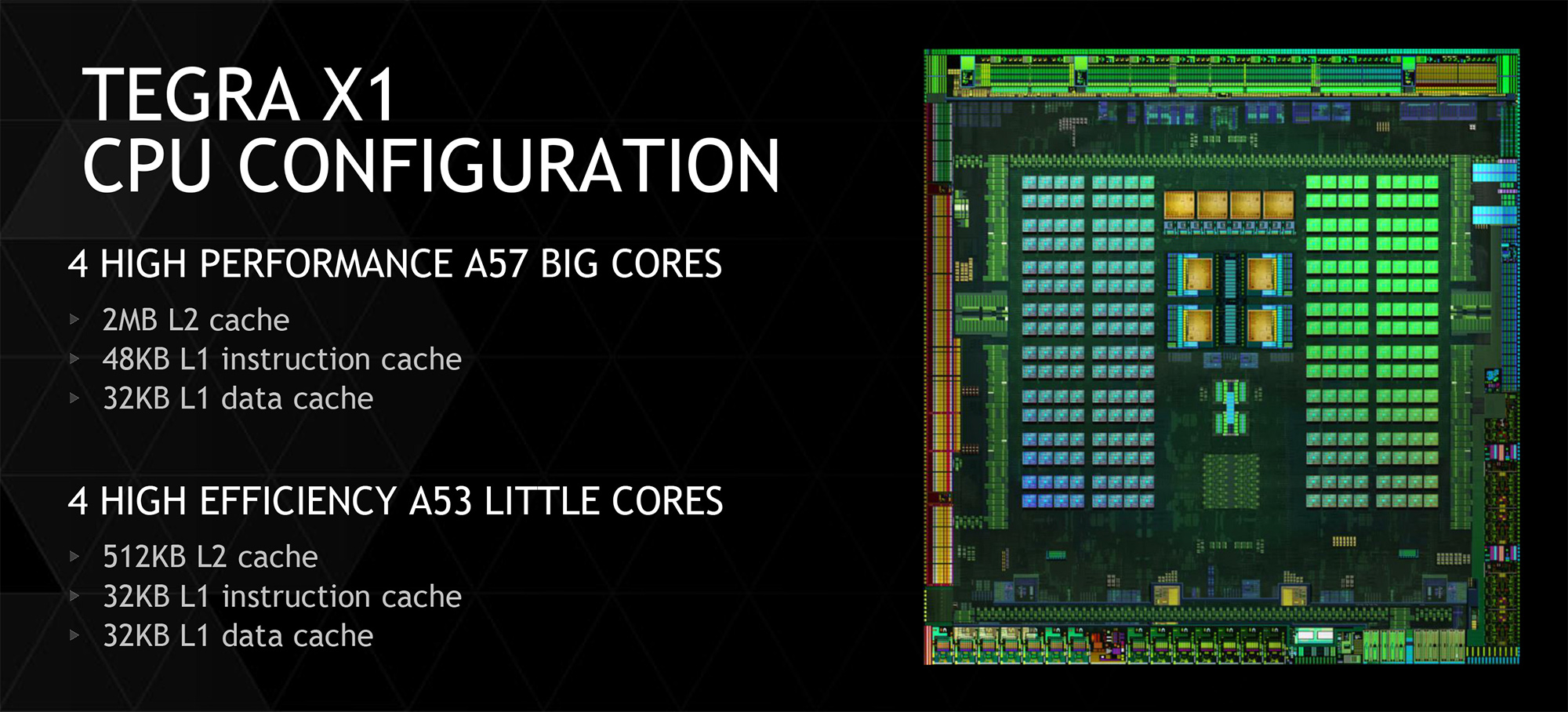
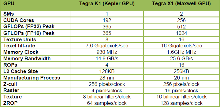
The all-new Nvidia Tegra X1 integrates four high-performance ARM Cortex-A57 cores with 512KB L2 cache, 48KB L1 instruction cache and 32KB L1 data cache per core as well as four low-power ARM Cortex-A53 cores with 128KB L2 cache, 32KB L1 instruction cache and 32KB L1 data cache per core. The latest system-on-chip from Nvidia also sports advanced graphics sub-system based on the Maxwell architecture that features 256 stream processors (two Maxwell stream multiprocessors), 16 texture units and 16 raster output pipelines that supports OpenGL ES 3.1, OpenGL4.5, DirectX 12.0 (feature level 11_3), and AEP application programming interfaces. The new SoC’s memory controller supports up to 4GB of LPDDR3 or LPDDR4 memory, whereas the AP’s storage controller supports eMMC 5.1 interface with CMD queuing. All other I/O interfaces are also present (see the diagram below).
Nvidia greatly improved multimedia capabilities of Tegra X1. The latest AP supports hardware decoding of video in all high-definition and ultra-high-definition (4K) formats at 60Hz, including VP9, H.265 (HEVC), H.264 and others. It can also encode H.264, H.265 4K video at 30fps and VP8 1080p video at 60fps. The chip also supports up to six camera inputs with up to 100MP sensors, which is one of the reasons why it has a lot of chances to win on the market of automobiles. Finally, the Tegra X1 has two display controllers that support 4K UHD outputs via HDMI 2.0 (with HDCP 2.2 technology) interface, something that can make the chip suitable for a wide range of media players.

“Tegra K1 set a new bar for GPU compute performance, and now just a year later Tegra X1 delivers twice that,” said Linley Gwennap, founder and principal analyst of the Linley Group. “This impressive technical achievement benefits both 3D graphics, particularly on devices with high-resolution screens, as well as GPGPU software that is becoming more prevalent, particularly in automotive applications.”
Unfortunately, the premium Tegra X1 chip for consumer electronics still does not support any kind of broadband technology. As a result, not a lot of smartphones and tablets will likely integrate it despite of vast performance and rich functionality.
The Nvidia Tegra X1 system-on-chip is made using 20nm system-on-chip process technology at Taiwan Semiconductor Manufacturing Co.
Nvidia said no word when it expects the new chip to emerge on the market inside finished products, but it is logical to expect this to happen this year. The company also did not reveal exact power consumption of the SoC, but said it is below 10W.
Discuss on our Facebook page, HERE.
KitGuru Says: Without any doubts, the new Tegra X1 is a mobile performance powerhouse. It has eight great general-purpose ARMv8 64-bit cores, it has a great graphics sub-system, it has serious image processing technology inside and it supports all major input/output interfaces everyone will need in the foreseeable future. For some reason, Nvidia decided not to touch upon its power consumption, which should not be too high given the 20SoC manufacturing technology, but not too low either due to high complexity. However, the company’s PR technologists decided to compare FP16 performance of Tegra X1 to FP64 performance of ASCI Red supercomputer, the world’s first 1TFLOPS supercomputer. The problem is that while FP16 is enough for certain graphics applications today (still, loads of apps use full FP32 precision), it is definitely not enough for any kind of high-performance computing applications. So, comparing FP16 performance to FP64 performance is clearly an apples to oranges kind of comparison. But an important thing is that Maxwell architecture was not designed for supercomputers, its FP64 rate is about 1/32 of its FP32 rate. So, if 256 SPs inside the Tegra X1 can offer 512GFLOPS at FP32, then its FP64 rate is 16GFLOPS. Not quite a teraflop, eh?
