
Today we are taking a look at the new Asus GTX 750 Ti, the third Maxwell card we have reviewed since Nvidia launched back on February 18th. So far we have analysed the MSI GTX750 Ti OC Twin Frozr and the Palit GTX 750 Ti StormX Dual – both fantastic solutions … so we will be interested to see how the Asus solution stacks up.
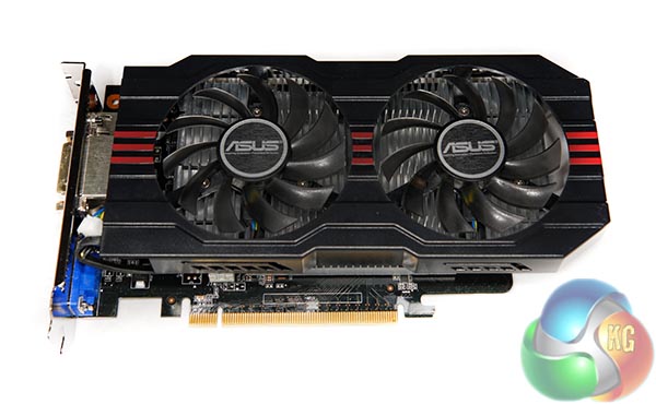
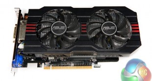
The new Asus GTX 750 Ti 2GB is a modified design featuring dual fans and enhanced out of the box clock speeds.
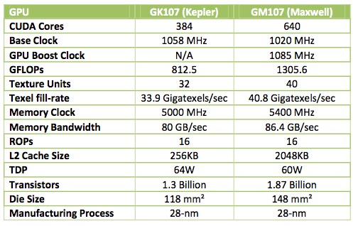
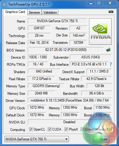
The Asus GTX 750 Ti receives a modest core clock increase, from 1,020 mhz to 1,072 mhz. Unlike the Palit GTX 750 Ti StormX Dual the memory is left at the default speeds of 1,350mhz (5.4Gbps effective). All cards have 16 ROP's, 53 TMU's and 640 CUDA cores.
The Nvidia reference card is using 2GB of Hynix GDDR5 memory, but ASUS have opted for Samsung branded GDDR5.
The Maxwell SM architecture delivers improved efficiency and 35% more performance per CUDA core on shader limited workloads. Nvidia have changed the architecture with the SM scheduler architecture and algorithms having been rewritten to avoid stalling and further reducing the energy per instruction required for scheduling. Maxwell SM architecture enabled Nvidia to increase the number of SM’s to five in GM107, compared to two in GK107 – and all with only a 25% increase in die area.
Nvidia have explained that the organisation of the SM has been changed. Each SM has been partitioned into four separate processing blocks, each with their own instruction buffer, scheduler and 32 CUDA cores. GK107 Kepler could have a non power of two number of CUDA cores, with some shared. The new partitioning simplifies the design and scheduling logic which reduces computation latency and saves area and power demand.
Pairs of processing blocks share four texture filtering units and a texture cache. The L1 compute cache function is now combined with the texture cache function and shared memory is a separate unit, shared across all four blocks. Each Maxwell SM is smaller than a Kepler SM but delivers around 90% of the performance. The smaller area means that Nvidia can incorporate many more SM’s per GPU. The GM107 (v GK107) has 25 percent more texture performance, 1.7 times more CUDA cores and 2.3 greater shader performance.
Nvidia have improved Video capabilities with the latest hardware. Maxwell incorporates an improved NVENC block to deliver faster encode performance over Kepler – 6-8 times real time compared against 4 times. Nvidia report a 8-10 times faster decode rate too. Maxwell also has a new GC5 power state designed to drop the GPU power demand under light workload situations – such as when playing back video.