
Last week AMD released their new R7 265 graphics card, and KitGuru was on hand to review the custom cooled Sapphire version. AMD tweaked their old HD7850 design and dropped the price to £100 in an attempt to dominate the market. Today we are looking at Nvidia's new budget grade enthusiast gaming card, the GTX 750 Ti.

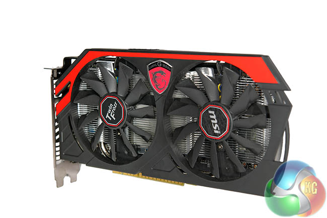
In this review we will be focusing on the MSI GTX 750 Ti OC Twin Frozr. This card has received the full ‘MSI treatment' – enhancing the reference design significantly with a two fan cooling system and improved heatsink. The MSI ‘OC' version is unsurprisingly clocked higher than the reference Nvidia design and we will discuss the changes shortly.
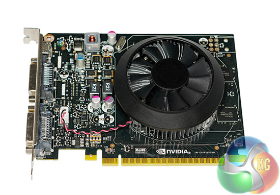
We did also receive a reference GTX 750 ti from Nvidia and while it isn't as exciting as the MSI version we will be including results from both cards in our tests today. Both solutions take all the power they need direct from the PCIe slot. If you have a really good memory, you will recall that the previous generation GTX650 Ti required power from an additional single 6 pin PCI E connector.
The GTX750 Ti is based around the Maxwell architecture which has been designed to enhance performance while optimising power efficiency per watt. The first Maxwell based GPU is codenamed GM107 and is designed for use in power limited environments such as notebooks and small form factor systems. Nvidia claim that the improvements in architecture mean that the GTX750 Ti will match the performance of their GTX480 flagship card from four years ago but with a TDP of only 60W. In real world terms, you get the same performance for only 25% of the power drain.
While the talking point of the Maxwell based GTX750 ti is primarily power efficiency, Nvidia do plan on releasing higher performance graphics cards using similar architecture at a later date.
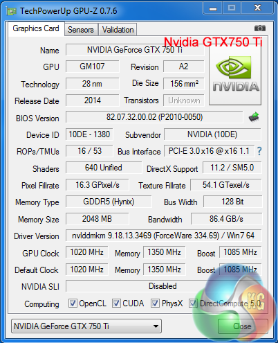
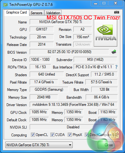
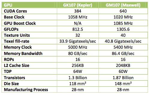
The GM107 GPU has a single GPC, five Maxwell Streaming Multiprocessors (SMM) and two 64 bit memory controllers (128 bit). The reference card is clocked at 1020mhz although MSI have overclocked their Twin Frozr version to 1,085mhz, with a boost speed of 1,163mhz. Both cards have 16 ROP's, 53 TMU's and 640 CUDA cores.
The Nvidia reference card is using 2GB of Hynix GDDR5 memory, but MSI have opted for Samsung branded GDDR5 – as we will see on the next page of the article today.
The Maxwell SM architecture delivers improved efficiency and 35% more performance per CUDA core on shader limited workloads. Nvidia have changed the architecture with the SM scheduler architecture and algorithms having been rewritten to avoid stalling and further reducing the energy per instruction required for scheduling. Maxwell SM architecture enabled Nvidia to increase the number of SM's to five in GM107, compared to two in GK107 – and all with only a 25% increase in die area.
Nvidia have explained that the organisation of the SM has been changed. Each SM has been partitioned into four separate processing blocks, each with their own instruction buffer, scheduler and 32 CUDA cores. GK107 Kepler could have a non power of two number of CUDA cores, with some shared. The new partitioning simplifies the design and scheduling logic which reduces computation latency and saves area and power demand.
Pairs of processing blocks share four texture filtering units and a texture cache. The L1 compute cache function is now combined with the texture cache function and shared memory is a separate unit, shared across all four blocks. Each Maxwell SM is smaller than a Kepler SM but delivers around 90% of the performance. The smaller area means that Nvidia can incorporate many more SM's per GPU. The GM107 (v GK107) has 25 percent more texture performance, 1.7 times more CUDA cores and 2.3 greater shader performance.
Nvidia have improved Video capabilities with the latest hardware. Maxwell incorporates an improved NVENC block to deliver faster encode performance over Kepler – 6-8 times real time compared against 4 times. Nvidia report a 8-10 times faster decode rate too. Maxwell also has a new GC5 power state designed to drop the GPU power demand under light workload situations – such as when playing back video.