The exact plans of Advanced Micro Devices and Nvidia Corp. concerning the 20nm process technology from Taiwan Semiconductor Manufacturing Co. have never been publicly revealed and are not completely clear at this point. One of the reasons for that are low manufacturing yields, which forces fabless semiconductor designers to reconsider their plans; another reason is concern about TSMC’s ability to make enough 20nm chips, which makes chip developers review their launch schedules. However, there seems to be yet another potential reason why there are no leaks about 20nm GPUs: a new media report claims that Nvidia has simply decided to skip the 20nm technology and use the 16nm FinFET tech next year instead.
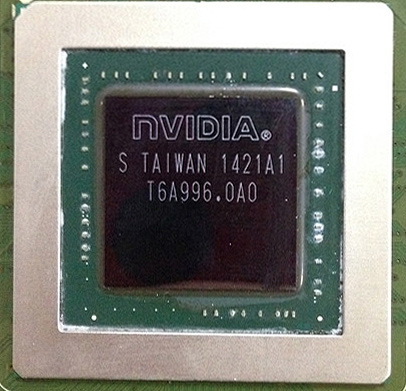
GM204: a mysterious GPU
VideoCardz web-site reports (citing a news-story from SemiAccurate web-site [which requires subscription]) that Nvidia plans to release the code-named GM204 graphics processing unit (which was previously known under the GM104 code-name) this October. Eventually four versions of the GM204-based GeForce GTX 800-series graphics cards with 1920 – 2560 stream processors (depending on the model) are expected to be available. The GM204 is projected to be made using 28nm fabrication technology. What is interesting is that Nvidia will reportedly skip the 20nm and will use 16nm fabrication process to make something that the media reports call the GM204b GPU.
Since TSMC’s woes with 20nm process technology were unexpected and the GM204 could have been redesigned to be made using 28nm process technology instead, its actual specifications and die size are unclear. If the chip integrates up to 2560 stream processors, is based on the Maxwell architecture and is made using 28nm fabrication process, then its die size should be over 500mm2. Increased efficiency of the new architecture should make the GM204 faster than the GK110, but not too dramatically, which is why it is uncertain why Nvidia wants to offer a new high-end solution that will not be significantly faster than the existing one.
If the GM204 is designed to replace the GK104 GPU, is made using 28nm process technology and features around 300mm2 die size, it cannot integrate up to 2560 stream processors. Moreover, it probably does not need that many SPs to leave the GK104 (which has 1536 stream processors) behind in terms of performance. Based on what we do know about the GM204, the chip is slightly bigger than the GK104.
TSMC’s 16nm looks better than the 20nm
TSMC’s 20nm fabrication process has always been a strange one. Typically foundries offer several versions of manufacturing technologies aimed at different application: high-performance-chips, low-power chips, low-cost chips, etc. In case of 20nm TSMC only offers only one version of the process aimed at everything from low-cost system-on-chips for ultra-portable devices (such as smartphones) to high-performance processors (such as GPUs). Since there are reports about low 20nm yields at TSMC, high prices and limited production capacities available to AMD and Nvidia, it may make sense not to use this fabrication technology and jump directly to 16nm, which is set to be available for commercial chips in early 2015.
While the 16nm FinFET process technology makes more sense to use in early 2015 than the 20nm manufacturing technology, there is another reason why Nvidia could be more interested in this technology. TSMC has already developed 16nm FinFET+ fabrication process that will be utilised to make chips in volume later in 2015. In fact, TSMC expects the majority of its customers to use the 16nm FinFET+ version of the process due to its noticeable benefits compared to the original. It is interesting to note that there is a rumour about yet another 16nm process technology from TSMC called 16nm FinFET turbo. So far TSMC has not confirmed the existence of the third 16nm FinFET process.
Design rules of the 16nm FinFET and the 16nm FinFET+ are the same, everything is largely compatible. In general, 16nm FinFET designs can easily be produced on the 16nm FinFET+ node with minimal changes (if needed at all). The “plus” process is expected be fully qualified by September. TSMC’s fabs compatible with the company’s 20nm process technology are 95 per cent ready to produce chips using various versions of the company’s 16nm manufacturing technology, the company said earlier this year/
According to TSMC, 16nm FinFET+ provides up to 15 per cent performance improvement over the 16nm FinFET at the same level of power consumption. At the same clock-rate, chips produced using 16nm FinFET+ are expected to consume 30 per cent less power compared to the same chips made using 16nm FinFET.
In general, once Nvidia designs a chip for the 16nm node, it can speed it up using either the 16nm FinFET+ technology or the rumoured 16nm FinFET turbo technology, which means that the company can easily refresh its 16nm product line in 2016 by spending almost nothing on the development.
GM204b: an even more mysterious GPU
While it makes sense to skip the 20nm fabrication process for Nvidia, it is doubtful that the 16nm fabrication process will be used to produce the GM204b graphics processing unit.
If the GM204 is designed to replace the GK104 GPU and features around 300mm2 die size, it will shrink to around 150mm2 size when produced using 16nm fabrication process. While the GM204b will most probably be very cost-efficient to make, it will be rather hard to route a 256-bit GDDR5 memory bus to such a small chip. Therefore, it is more likely that Nvidia’s first 16nm GPU will be different from a simple GM204 redesigned for a different process technology.
If the GM204 is needed to replace the GK110 this year (which, as we know, it will not), then shrinking its die size from circa 500mm2 next year to around 250mm2 (in case of the GM204b) and reducing its price makes a lot of sense. However, that would create a mess on the market since there will be products with similar performance made using different process technologies and available at different price-points.
Final words
While Nvidia can theoretically skip the 20nm process technology and start to use the 16nm FinFET and derivatives, it will unlikely just redesign anything released on the 28nm node and produce it using the 16nm process technology (at least, not for the desktop market). Keeping in mind the advantages that the 16nm process technologies provide, it is more likely that Nvidia will try to release two brand-new generations of products made using 16nm FinFET and 16nm FinFET+ manufacturing processes. The company did something like that before with two generations of Fermi GPUs. If Nvidia follows such hypothetic plan, it will probably have three generations of the Maxwell-based products.
Nvidia did not comment on the news-story.
Discuss on our Facebook page, HERE.
KitGuru Says: While unofficial information cannot be fully trusted, in many cases it is partly correct. While we do not know for sure whether Nvidia plans to skip TSMC’s 20nm node, we may assume that the company is not really impressed with the technology, which is why it may try to minimize its usage.