
Nvidia Corp. on Tuesday introduced its first graphics processing units (GPUs) based on code-named Maxwell architecture, which once again increases performance while minimizing power consumption. The initial graphics solutions based on the first-generation Maxwell are Nvidia GeForce GTX 750 Ti and GeForce GTX 750.
To boost performance per stream processor and per watt, Nvidia had to change internal architecture of graphics processing units once more with the first generation Maxwell architecture. To do so, Nvidia dumped the large SMs [streaming multiprocessors] of Kepler GPUs with complex control logic and 192 stream processors per each. Instead, the firm introduced an SM divided into four blocks with own control logic (instruction buffer, warp scheduler, dispatch unit), register file and 32 stream processors per block. Each Maxwell SM features its own PolyMorph Engine 2.0 unit (one vertex fetch, one tessellator, one viewport transform, one stream output, etc.). Thanks to better programmability of each block within SM and higher utilization rate of each stream processors, Nvidia increased the peak performance per core by 35% when compared to the cores in its chips built with the previous generation Kepler architecture.
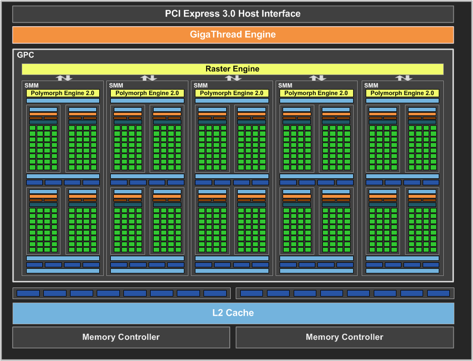
Block diagram of Nvidia GeForce GTX 750 Ti (GM107) graphics processor
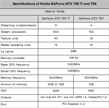
Since lower number of stream processors is needed to get certain amount of compute performance with Maxwell-based GPUs, less power is needed compared to the Kepler architecture. For example, the GeForce GTX 750 Ti only has 640 stream processors, yet, based on Nvidia’s own performance tests, it provides two times higher performance compared to the GeForce GTX 650 Ti with 768 stream processors. Moreover, power consumption of the GeForce GTX 750 Ti is just 60W.
“We know that to advance performance, we must advance performance per watt, because every system we design for has a power limit — from supercomputers to PCs to smartphones,” said Scott Herkelman, general manager of the GeForce business unit at Nvidia. “That's why we architected Maxwell to be the most efficient GPU architecture ever built.”
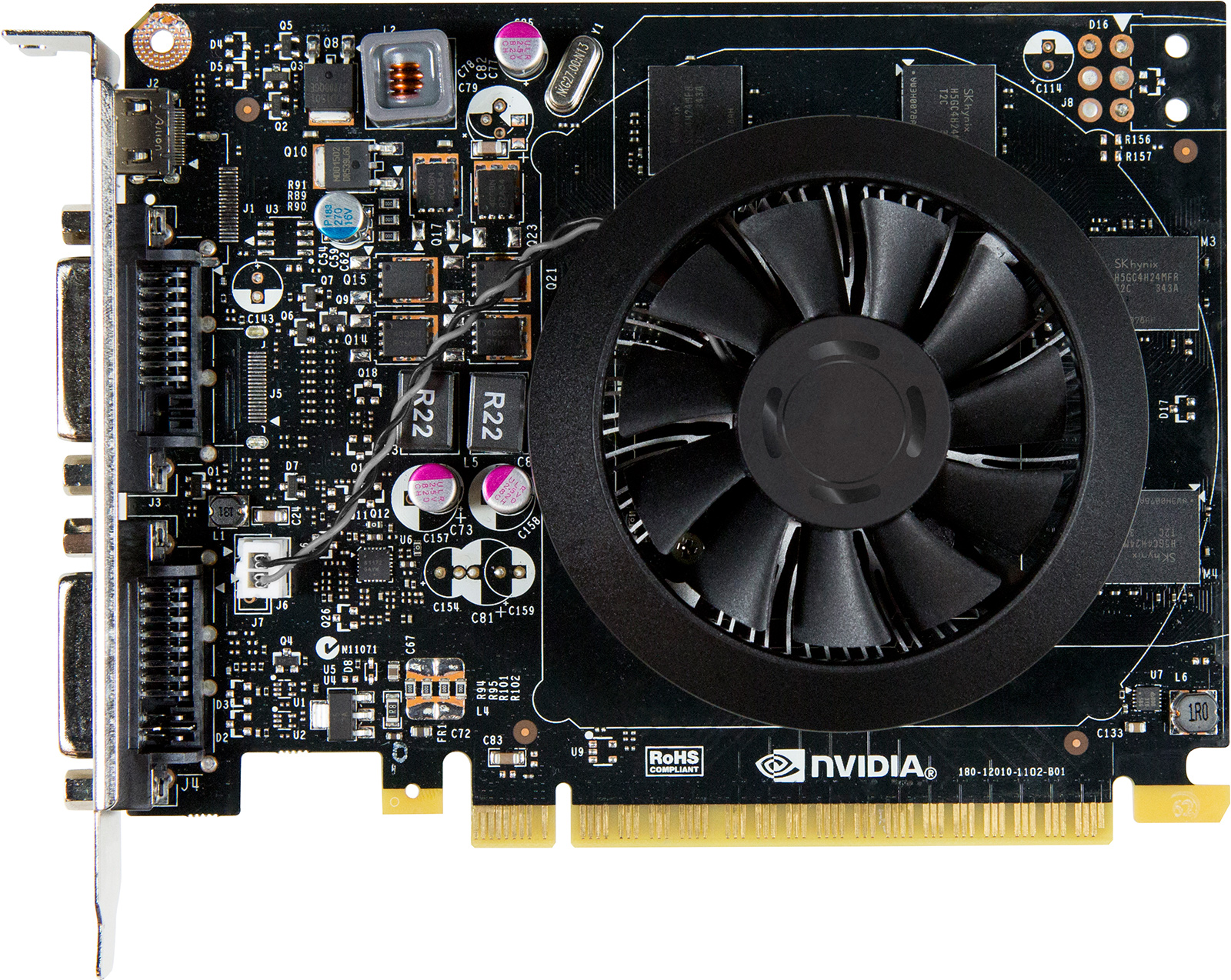
Nvidia GeForce GTX 750 Ti graphics card
The first graphics processing unit based on the first-generation Maxwell architecture is code-named GM107. The GPU has 5 SMs, 640 stream processors, 40 texture units, 16 raster operating units, 2MB L2 cache as well as 128-bit memory controller. The chip is made using 28nm process technology and contains 1.87 billion transistors. The first two graphics cards based on the GM107 are GeForce GTX 750 Ti and GeForce GTX 750.
Just like all mainstream graphics processors these days, Nvidia GM107 supports all modern graphics and GPU compute technologies, including DirectX 11, OpenGL 4.3, OpenCL 1.1 and others. In addition, the GM107 and systems on its base support a host of proprietary Nvidia technologies like PhysX, ShadowPlay, G-Sync, GameStream and some others.
The Nvidia GeForce GTX 750 Ti and GTX 750 GPUs are now available from the leading add-in card suppliers, including Asustek, Colorful, EVGA, Gainward, Galaxy, Gigabyte, Innovision 3D, MSI, Palit, PNY and Zotac. Pricing is expected to start at $119 for the GTX 750, $139 for the 1GB GTX 750 Ti and $149 for the 2GB GTX 750 Ti.
KitGuru Says: Maxwell seems to be rather efficient in terms of architecture, based on initial performance numbers. But what about high-end GPUs based on Maxwell? What about new features? It seems like we still do not have DirectX 11.2 here or any other improvements over the previous-generation Kepler architecture.