

The folks at the Samsung Advanced Institute of Technology have been busy collaborating with scientists from the Ulsan National Institute of Science and Technology, resulting in the discovery of a new material for semiconductors. Importantly, this discovery has the potential to “accelerate the advent of next generation semiconductors”.
The material in question is amorphous boron nitride (a-BN), which consists of boron and nitrogen atoms with an amorphous molecule structure. Samsung says that the new material has the “best-in-class ultra-low dielectric constant of 1.78” and has been demonstrated to grow on a wafer scale at a “low temperature of just 400°C”. Amorphous boron nitride is expected to be used for semiconductors in DRAM and NAND solutions, especially those who are targeted for large-scale servers.
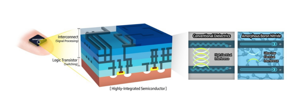
Image credit: Samsung
“To enhance the compatibility of graphene with silicon-based semiconductor processes, wafer-scale graphene growth on semiconductor substrates should be implemented at a temperature lower than 400°C.” said Hyeon-Jin Shin, a graphene project leader and Principal Researcher at SAIT. “We are also continuously working to expand the applications of graphene beyond semiconductors.”
Additional information about the new material can be found HERE.
Kitguru says: It's exciting when researchers discover a new material that can be used to propel technology even further.