
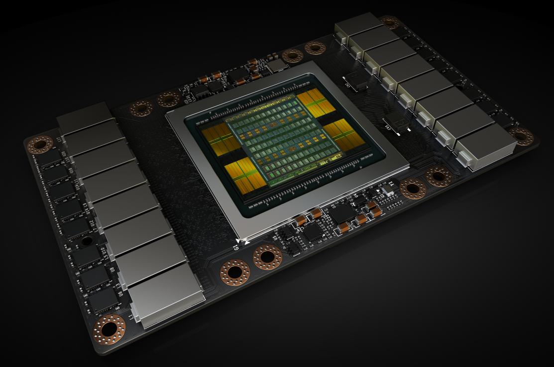
Today Nvidia kicked off the GPU Technology Conference, with CEO Jen-Hsun Huang taking the stage to announce its very first GPU based on the Volta architecture- the Tesla V100. This is the most advanced accelerator ever built, powered by 5120 CUDA cores, over 21 billion transistors and 16GB of HBM2 running at 900 GB/s.
The GV100 includes 21.1 billion transistors in total with a die size of 815 mm2. It is fabricated on a new TSMC 12nm FFN high performance manufacturing process. In all, it is a considerable jump in compute performance compared to the Pascal GP100.
To improve FP31 and FP64 performance, Nvidia has equipped the GV100 with a new SM Processor architecture. The new Volta SM is 50 percent more energy efficient than the Pascal design. On top of that, Volta is equipped with new ‘Tensor Cores', which are designed specifically to deliver up to 12 times higher TFLOPs for Deep Learning applications.
When it comes to memory, Nvidia has opted to go with Samsung's HBM2 modules, combined with a next generation memory controller in Volta. This combination provides 1.5 times more memory bandwidth when compared to the GP100. Volta's HBM2 implementation is also said to be around 95 percent more efficient when running under certain workloads.
Here are the peak computation units for the Tesla V100:
- 7.5 TFLOP/s of double precision floating-point (FP64) performance;
- 15 TFLOP/s of single precision (FP32) performance;
- 120 Tensor TFLOP/s of mixed-precision matrix-multiply-and-accumulate.
And finally, here is a table going over the full V100 spec compared to the last few generations of Tesla flagships.
| Tesla Product | Tesla K40 | Tesla M40 | Tesla P100 | Tesla V100 |
|---|---|---|---|---|
| GPU | GK110 (Kepler) | GM200 (Maxwell) | GP100 (Pascal) | GV100 (Volta) |
| SMs | 15 | 24 | 56 | 80 |
| TPCs | 15 | 24 | 28 | 40 |
| FP32 Cores / SM | 192 | 128 | 64 | 64 |
| FP32 Cores / GPU | 2880 | 3072 | 3584 | 5120 |
| FP64 Cores / SM | 64 | 4 | 32 | 32 |
| FP64 Cores / GPU | 960 | 96 | 1792 | 2560 |
| Tensor Cores / SM | NA | NA | NA | 8 |
| Tensor Cores / GPU | NA | NA | NA | 640 |
| GPU Boost Clock | 810/875 MHz | 1114 MHz | 1480 MHz | 1455 MHz |
| Peak FP32 TFLOP/s* | 5.04 | 6.8 | 10.6 | 15 |
| Peak FP64 TFLOP/s* | 1.68 | 2.1 | 5.3 | 7.5 |
| Peak Tensor Core TFLOP/s* | NA | NA | NA | 120 |
| Texture Units | 240 | 192 | 224 | 320 |
| Memory Interface | 384-bit GDDR5 | 384-bit GDDR5 | 4096-bit HBM2 | 4096-bit HBM2 |
| Memory Size | Up to 12 GB | Up to 24 GB | 16 GB | 16 GB |
| L2 Cache Size | 1536 KB | 3072 KB | 4096 KB | 6144 KB |
| Shared Memory Size / SM | 16 KB/32 KB/48 KB | 96 KB | 64 KB | Configurable up to 96 KB |
| Register File Size / SM | 256 KB | 256 KB | 256 KB | 256KB |
| Register File Size / GPU | 3840 KB | 6144 KB | 14336 KB | 20480 KB |
| TDP | 235 Watts | 250 Watts | 300 Watts | 300 Watts |
| Transistors | 7.1 billion | 8 billion | 15.3 billion | 21.1 billion |
| GPU Die Size | 551 mm² | 601 mm² | 610 mm² | 815 mm² |
| Manufacturing Process | 28 nm | 28 nm | 16 nm FinFET+ | 12 nm FFN |
KitGuru Says: Volta is officially here and it seems that Nvidia has made some interesting advancements with this new architecture. This is an interesting first look at what's to come later down the line too, though there will be some differences when Volta comes to the GeForce line, including a change from HBM2 to GDDR6 memory.