

Rambus has announced a new addition to its range of High-speed memory interface solutions with a new High Bandwidth Memory 2E controller and a physical layer IP to deliver maximum performance in a compact, power-efficient package.
The new HBM2E controller and PHY IP from Rambus provides customers with a complete solution to integrate HBM2E memory into products. The Rambus HBM2E interface is fully compliant with JEDEC HBM2E JESD235 standards and supports data transfer rates of up to 3.2 Gbps per data pin, via eight independent channels, containing 128 bits per channel for a total 1024 bits data width.
This configuration results in a total bandwidth of 410 GB/s per stack, from stacks of 2, 4, 8 or 12 DRAMs. The Rambus HBM2E interface is designed with an interposer to route signals between the DRAM stack and the PHY IP on the SoC. To ensure all power efficiency and thermal requirements are met, Rambus has undertaken complete signal and power integrity analysis on the entire system.
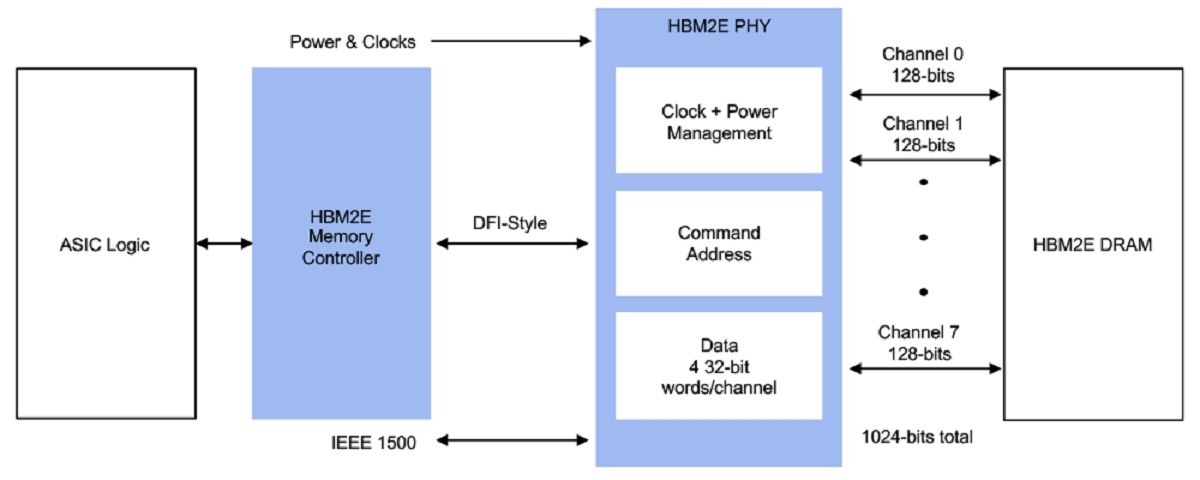
A co-verified Northwest Logic controller supports standard channel densities of up to 24 Gb while maximising memory bandwidth and minimising latency through Look-Ahead command processing. Combined with the HBM2E PHY, the HBM2E controller creates a complete HBM2E memory interface subsystem. Rambus also offer these products separately to be used with 3rd party HBM2E controllers or PHY solutions.
Discuss on our Facebook page HERE.
KitGuru says: This new HBM2E interface from Rambus offers developers of bandwidth-hungry ASICs an all-in-one solution that will save time and costs for companies implementing support for HBM2E memory into their designs.
