 KitGuru KitGuru.net – Tech News | Hardware News | Hardware Reviews | IOS | Mobile | Gaming | Graphics Cards


AMD is reportedly considering TSMC's A14 lithography node for its next-generation Zen 7 processor architecture. According to a recent report, the company has begun early supply chain preparations for the next-generation CPU architecture, following the high-volume production of its 2nm-based Zen 6 EPYC “Venice” server processors.
The report originates from Taiwanese media outlet Commercial Times (via Wccftech). For physical assembly, AMD is apparently exploring alternatives to TSMC by evaluating advanced packaging technologies from outside vendors such as Powertech. The report indicates that AMD is evaluating Fan-Out Panel-Level Packaging (FOPLP) solutions. The report also adds that this evaluation is being conducted alongside the development of next-generation 3D V-Cache implementations for the flagship Zen 7 product lines.
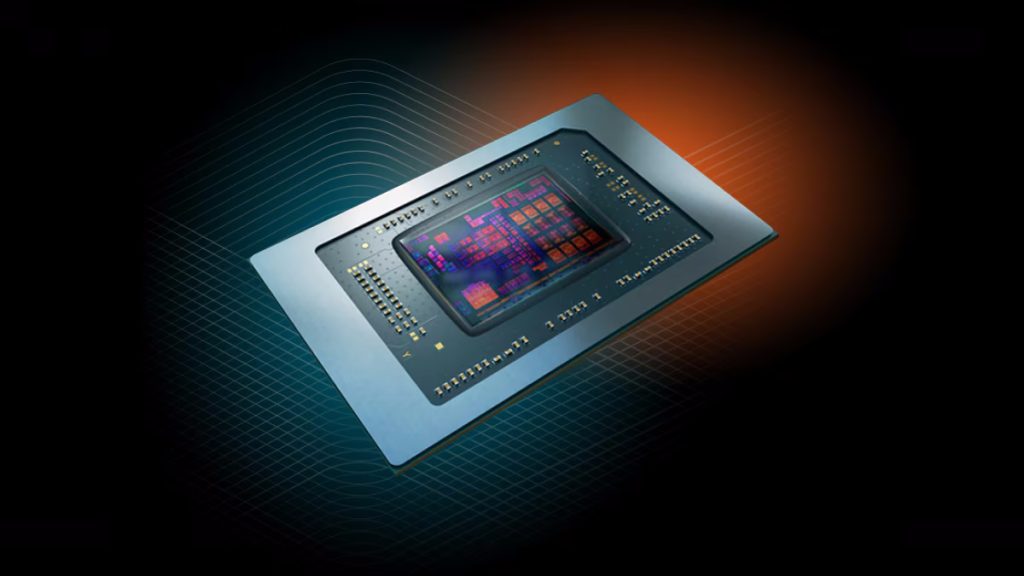
It is claimed that Zen 7 will increase AI processing efficiency and feature up to 16-cores per CCD. Other improvements may include the integration of AVX10, which combines AVX-512 and AVX2 vector math features, and AI Compute Extensions (ACE), an industry-standard instruction set designed to accelerate matrix multiplication workloads.
There is no word yet on when the first Zen 7 CPUs will launch, but they aren't expected until 2028.
Discuss on our Facebook page, HERE.
KitGuru says: Zen 7 is still quite a way off from hitting the consumer market, so plenty can change between now and then.