

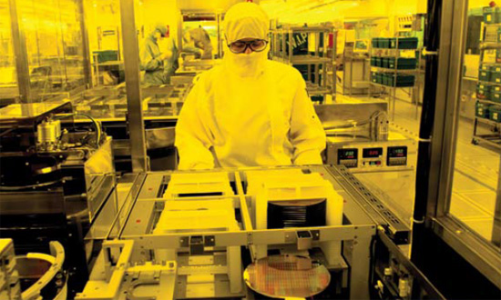
Samsung Electronics, one of the world’s top makers of NAND flash memory, last week announced that its new memory fab in Xi’an China has begun full-scale manufacturing operations. The new facility will produce Samsung’s advanced NAND flash memory chips, such as 3D V-NAND.
Vertical NAND (V-NAND) memory stacks memory cells vertically and uses a charge trap flash architecture. The vertical layers allow larger areal bit densities without requiring smaller individual cells, which means higher reliability and performance. According to Samsung, its V-NAND exhibits between two to ten times the reliability (endurance) and writes data (tPROG, program time) at least twice as fast as multi-level-cell (MLC) type planar NAND flash memory, while consuming half the power.
Production of 24-layer 128Gb V-NAND chips started last August in Hwaseong, Korea. The new facility will give Samsung an ability to boost production cost-efficiently.
By starting operations of its Xi’an fab, Samsung has secured a solid memory production base in China, a market where approximately 50 per cent of global NAND flash is generated from production bases operated by many IT companies here. The company will now be better positioned to serve its clients among makers of solid-state drives, smartphones, tablets and other devices that use NAND flash memory. It is very important that the new fabrication line is designed to produce stacked 3D V-NAND memory solutions, which are set to become popular in the coming years.
At present exact production capacities of the Xi’an facility are unclear, but a dedicated facility to produce advanced 3D V-NAND already means that the company is extremely serious about the new high-capacity memory chips for solid-state drives and other NAND flash-based applications.
The new fab is also laying the basis for a more stable supply of memory products to Samsung’s clients. The company plans to complete construction of its entire Xi’an complex, which includes an assembly facility and test line, by the end of this year.
Construction of the new manufacturing facility took 20 months since Samsung broke ground here in September, 2012. The total area of the facility is approximately 230,000 square meters, situated on 1.14 million square meters of land.
Discuss on our Facebook page, HERE.
KitGuru Says: 3D V-NAND memory is a major breakthrough in NAND flash manufacturing. Keeping in mind that at present only Samsung produces it, the start of the Xi’an operations shows how far ahead Samsung is from its rivals.