

Nvidia Corp. and its partners among makers of graphics cards are expected to release the next-generation GeForce GTX 800-series solutions sometimes in October (or even late September), according to multiple reports. But while the new graphics solutions are just a couple of months away, it is completely unknown what to expect from them. We decided to analyze what we do know for sure about the GM204, the graphics processor that will power the new cards, and what kind of specifications and performance should we expect.
Facts we know for (almost) sure
While there are not a lot of reliable facts from sources close to Nvidia available at the moment, here is what we have found so far about the GM204 and what either is trustworthy or, at least, looks trustworthy:
- Nvidia GM204 is based on the code-named Maxwell architecture;
- Nvidia GM204 is made using 28nm process technology (given that multiple sources said that the GM204 is a 28nm GPU, it is most probably a fact);
- Nvidia GM204 has die size of around 300mm² (we’ve seen the chip, we’ve discussed that performance GPUs from Nvidia feature about 300mm² die size);
- Nvidia GM204 most likely 256-bit memory bus (we’ve seen a GM204-based card, it features 16 GDDR5 memory chips (with 16-bit or 32-bit interfaces), hence, given the size of the chip, 256-bit memory bus is a more likely option);
While we have no idea about exact specifications of the GM204, we do know specifications of the GM107 thanks to the official launch of the GeForce GTX 750-series GPUs earlier this year and hence we know something about the Maxwell architecture in general.
Maxwell architecture
Nvidia’s graphics processors consist of several key building blocks: main scheduler/dispatch processor (which Nvidia calls GigaThread Engine), GPCs [graphics processing clusters], SMMs [streaming multiprocessor module], ROPs [raster operating units], cache, memory controllers.
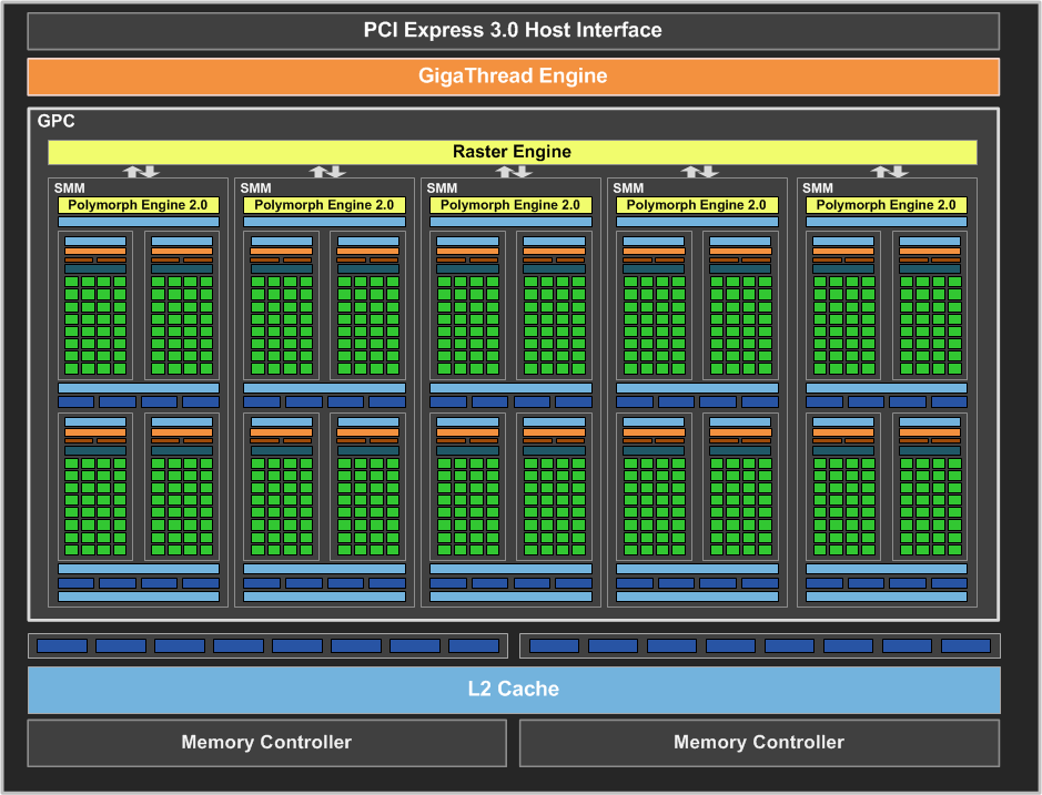
A block diagram of Nvidia's GM107 graphics processing unit.
The GM107 graphics processor based on the first-gen Maxwell architecture features one GPC unit, 16 ROPs (in two blocks,), 2MB L2 cache and two 64-bit memory controllers. The GPC of the GM107 consists of five SMMs. Each first-gen Maxwell SMM features its own PolyMorph Engine 2.0 unit (one vertex fetch, one tessellator, one viewport transform, one stream output, etc.) and is divided into four blocks with their own control logic (instruction buffer, warp scheduler, dispatch unit), a register file, two texture units (TUs) and 32 stream processors (SPs) (thus, each SMM features 128 SPs, 8 TUs, etc.).
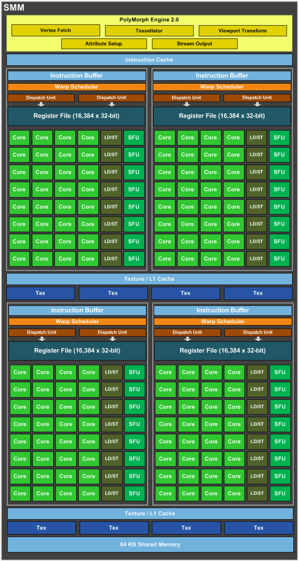
A block diagram of a Maxwell SMM
According to Nvidia, thanks to better programmability of each block within an SMM and higher utilization rate of each stream processors, the company increased the peak performance per stream processor by 35% when compared to the SPs in its chips built with the previous generation Kepler architecture. Therefore a Maxwell-based GPU with equal (or more or less equal) amount of stream processors with a Kepler-based GPU will perform around 35 per cent better.
Nvidia’s GM107 graphics processing unit features 640 SPs, 40 TUs, 16 ROPs, 2MB cache and a 128-bit memory controller. The chip contains 1.87 billion of transistors and has 148mm² die size.
What Nvidia needs from GM204?
Since the GM204 is a successor to the GK104 graphics processor (GeForce GTX 670, 680, 760 and 770) made using the same 28nm process technology, Nvidia cannot really expect it to outperform its predecessor by two times or something like that. Realistically, Nvidia needs to tangibly outperform the best GK104 by around 30 to 40 per cent. It is impossible that a 300mm² Maxwell chip could beat the GK110 GPU with 2880 stream processors (which die size is 551mm²), hence, it is not a target that the GM204 should achieve.
Possible GM204 configurations
Each architecture can be scaled to offer better performance or lower power consumption. Let’s try to assume how Nvidia could scale the GM107’s architecture to offer better performance with the GM204 while maintaining around 300mm² die size.
The easiest way to double performance of the GM107 is to double the amount of virtually everything inside: GPC, ROPs, cache, memory controllers. Such a chip would have 1280 stream processors, 80 texture units, 32 ROPs and a 256-bit memory bus. The GPU would never outperform the GK104 (1536 SPs, 128 TUs, 32 ROPs, etc.) significantly and in many cases will be behind the older solution. Therefore, it is unlikely that Nvidia will take this route. Moreover, such a chip would be significantly smaller than 300mm² since not all elements of the chip have to be doubled.
What Nvidia did with GK110 compared to the GK104 architecturally (at least when it comes to organization of execution units) was the increase of the amount of SMs [streaming multiprocessor] per GPC from two to three. The same approach could be used for the GM204 too. Nvidia could expand GPC to six SMMs and then double the amount of GPCs (and ROPs, cache, memory controllers) per chip. Such a GPU would feature 1536 SPs, 96 TUs, 32 ROPs as well as a 256-bit memory bus and could offer up to 35 per cent higher performance compared to the GK104 at the same clock-rate. The die size of such chip would probably be around 300mm², but since we do not know anything about exact sizes of the GM107’s elements, we cannot be 100 per cent sure.
Theoretically, Nvidia could put six blocks into each SMM (thus increasing the amount of SPs per SMM to 192), then double the amount of GPCs (along with ROPs, cache, memory controllers) per GPU. If Nvidia manages to do this, then the final chip would feature 1920 SPs, 120 TUs, 32 ROPs and a 256-bit memory controller. Would that all fit into a 300mm² die area? Possibly. However, since this fundamentally changes the architecture of the SMM, this could also affect efficiency of Maxwell architecture in general. Therefore, the expansion of GPC to seven SMMs (and doubling the amount of GPCs, etc.) sounds more realistic (the GPU would have 1792 SPs, 112 TUs, 32 ROPs, 256-bit memory bus).
Final words
While chip designers can do many unexpected things and sometimes even wonders, they cannot overrule the laws of physics. Engineers will not be able to squeeze 3200 stream processors into the GM204 that is made using 28nm process technology and has die size of around 300mm². Therefore, the most logical configurations of the fully-fledged GM204 (the GeForce GTX 880) are as follows:
- 1536 SPs, 96 TUs, 32 ROPs, 256-bit memory bus
- 1792 SPs, 112 TUs, 32 ROPs, 256-bit memory bus
- 1920 SPs, 120 TUs, 32 ROPs, 256-bit memory bus
Of course, these specifications may be wrong as well…
Nvidia did not comment on the news-story.
Discuss on our Facebook page, HERE.
KitGuru Says: Keep in mind that this news-story is highly speculative. We do not know exact sizes of Maxwell’s SMM, GPC and the un-core, therefore, take everything with a grain of salt. Nvidia has never revealed a die shot of the GM107 probably for a reason. Otherwise, it would be relatively easy to model the GM204.

No I’ll wait for official those specs are horrible
I have a GTX 650 Ti OC ! i will wait for post launch analysis. Lets see what Gen 2 Maxwell have in it.
I’m expecting this card to be a decent bit faster than the 780 that it’s replacing, and maybe even faster than the more expensive Kepler cards. If it’s not, then I’ll be holding out for the 9XX cards.
I need to replace my 670 anyways. I replace my GPU every 2-3 series depending on the jump.
The die is approx 430mm2 not 300mm2. Someone counted the pixels and compared with GK104 and GK110. Its bigger than GK104 and smaller than GK110.
hmm this spec just to trow AMD off…
Nvidia is not saying anything until the last day of gamescon
If those specs are right then the 780 Ti is still going to outperform the 880 minus maybe some extra vram
RUBBISH!
First of all its not going to be 300mm.
Secondly if it doesn’t outperform the GTX 780 ti, the whole 800 series is a complete moot, why would anyone bother and not just wait for the 900 series or inevitable Ti variants.
I’m pretty sure its going to pack 3200 cores and outperform the GTX 780ti just enough for it to be a viable single card solution.
28nm? Don’t need new GPU 760 is doing perfect, if the next series don’t directly jump to 16nm, won’t get it either. Don’t want to watch that Asian guy bragging about himself, and what miracles nVidia have achieved even if it’s bs
Plot twist -> GM204 using 20nm, hence 3200 SPs in 300mm sq die size make perfect sense.
This is the only way to explain the FSE score of 6K plus, and NV has never release a GTX x80 card that is slower than previous x80. So it make logical sense that GTX 880 cannot be slower than GTX 780