

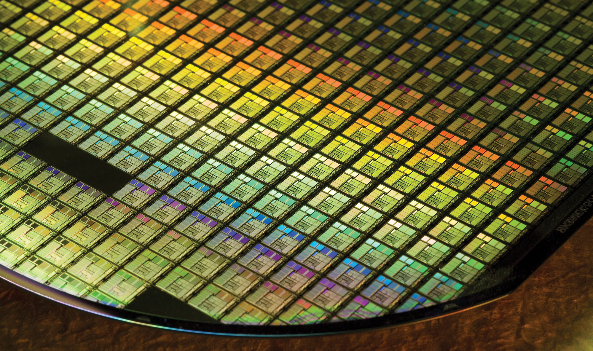
Taiwan Semiconductor Manufacturing Co. this week disclosed some additional details about its 7nm fabrication process. TSMC reiterated plans to start qualifications of the technology in early 2017 and then initiate volume production in 2018. The 7nm process will use certain elements derived from the 10nm fabrication process, which will help the company and its clients in terms of yields and transition, but with trade-offs.
7 in 18
“The development activity on our 7nm is also ongoing with full steam,” said said Mark Liu, president and co-CEO of TSMC, during the company’s earnings conference call with investors and financial analysts. “We have a parallel team working on that program. We target 7nm technology qualification in the first quarter 2017, only five quarters after 10nm.”

Typically, it takes a year for foundries to start volume production after they initiate risk production using a particular process technology. While the time-to-market of TSMC’s 7nm fabrication process seems to be rather phenomenal — first half of 2018, it should be noted that the tech will not be something completely new, designed from scratch. According to Mr. Liu, the 7nm manufacturing technology (which official name remains unknown) will have a “relationship” with 10nm similar to that between TSMC’s 16nm and 20nm processes.
Relationship
The high-ranking executive did not elaborate about the nature of the “relationship”, but said that it would allow chip developers to keep using the same chip manufacturing process tools (e.g., defect inspection, review, metrology, lithography modeling tools, etc.) as with the 10nm process. Moreover, experience that TSMC will have with its 10nm process tech will help it to improve yields at 7nm.
“For 7nm, similar to our 20nm and 16nm relationship, we are developing 7nm to be able to leverage the process tool compatibility and maturity from 10nm volume production,” said Mr. Liu.
TSMC’s 16nm manufacturing technologies use planar back-end-of-line (BEOL) interconnect flow originally designed for the company’s 20nm process. As a result, die sizes of chips produced at 16nm node are not smaller than those of ICs [integrated circuits] made using 20nm tech. While TSMC’s 16nm processes help chip developers to greatly improve performance vs. 20nm technology, relatively low transistor density of the processes make them rather expensive since any substantial increase of transistor budget (vs. real or hypothetical 20nm device) directly affects costs. On the other hand, re-use of BEOL ensures relatively high yields already early in the life-cycle of the tech.
Scaling under question
TSMC did not reveal any actual details about its 7nm technology. Officially, the company promises that the tech will enable frequency increase and “chip scaling”, but if it re-uses BEOL originally designed for 10nm process, geometry scaling cannot be significant. On the other hand, since 10nm fabrication process does not provide a really significant performance improvement compared to 16nm FinFET+ technology, 7nm is just what the doctor ordered for high-performance designs.
“With further transistor speed enhancement and chip scaling from 10nm, our customer can plan their tape-outs using the latest and the greatest technology available at the time when they launch their most competitive products,” said the president and co-CEO of the company.
New realities
Back in the days TSMC and UMC introduced optical shrinks (or half-nodes) of their process technologies that used similar libraries, EDA tools and manufacturing equipment, but featured smaller sizes of elements because foundries tweaked optical components of their scanners to “draw” finer “lines”. This helped to reduce costs of chips, slightly increase their clock-rate potentials and/or lower power consumptions without using all-new process technologies and necessity to redesign chips from scratch.
Nowadays, optical shrinks are no longer used. However, it is possible to use similar flows across multiple generations of fabrication technologies. TSMC, Samsung and GlobalFoundries re-use 20nm BEOL with their 16nm and 14nm manufacturing processes. This helps to avoid a number of problems and bring new technologies to market faster. However, it also means that “truly” new production processes that scale everything – transistor density, frequencies, power consumption, etc. – do not emerge very often nowadays.
In fact, Intel remains the only company, which develops new manufacturing technologies with the aim to improve every aspect of its chips. Unfortunately, it takes a long time to design such leading-edge processes. Based on various comments made by Intel recently, the chip giant intends to consider using new materials, new transistor structures and extreme ultraviolet (EUV) lithography for its 7nm fabrication technology.
Discuss on our Facebook page, HERE.
KitGuru Says: With “hybrid” approach to process technology development, the number of nanometres in the name of the process just becomes irrelevant. While this has been true for quite a while, in the coming years it will just get too evident.

Yes, a Company which isn’t capable of offering 16nm finfet products in the third Quarter of 2015, wants to release 16nm finfet + after this, and then 10nm, and after that 7nm in…. YES… 2018.
Great.
->
>
Hey big mouth tsmc first release 16 nm chip then think about 7nm