

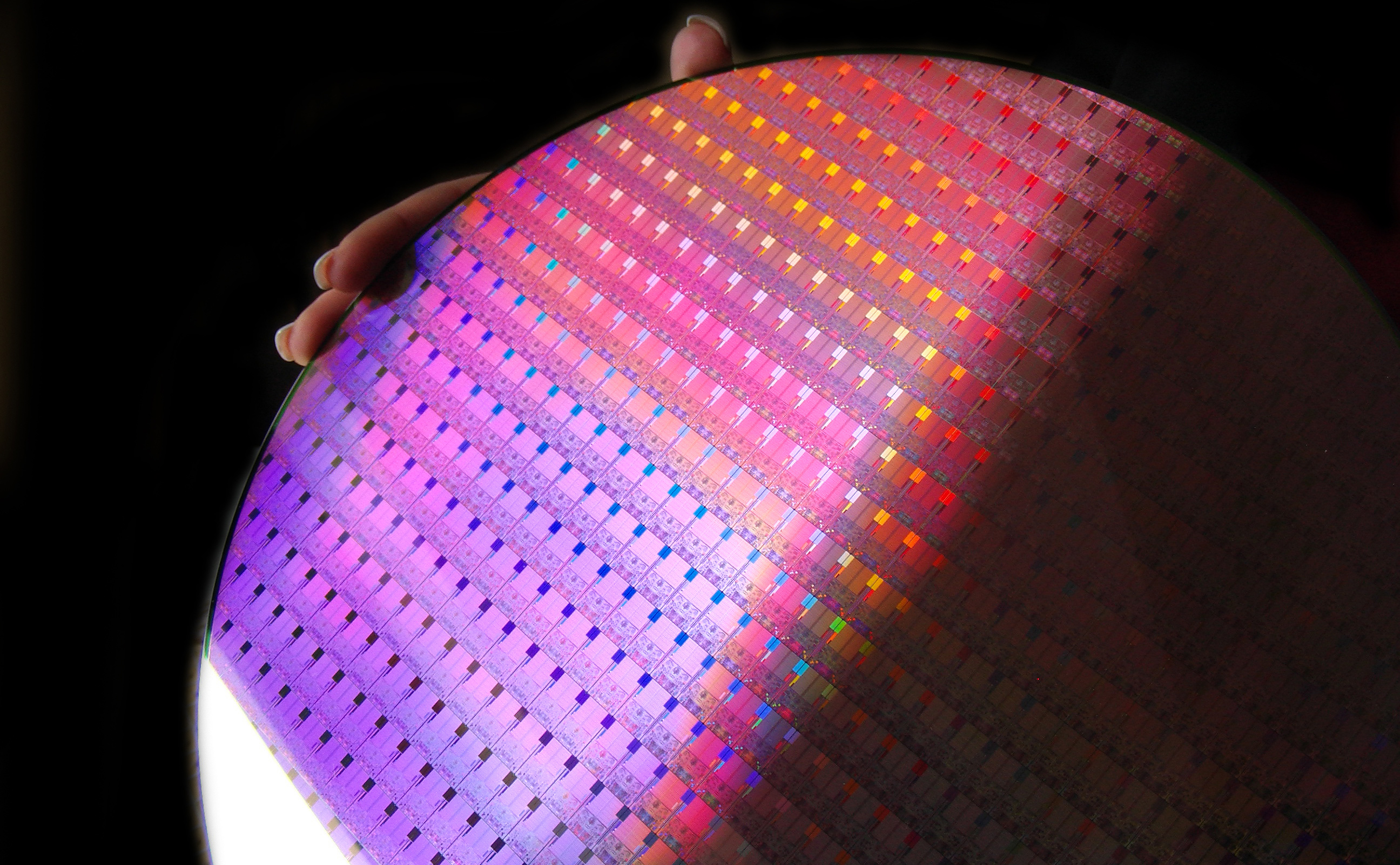
Intel Corp. on Wednesday confirmed the delay of mass production of central processing units using 10nm fabrication process to 2017. The company said that it ran into difficulties with its 10nm technology and decided to stretch the life-cycle of 14nm process with one more family of CPU products code-named “Kaby Lake”. Intel admitted that it now takes about 2.5 years to transit from one manufacturing technology to another, which means the stretch of Moore’s law cadence.
When Gordon Moore first did his observation regarding doubling the number of transistors in an integrated circuit in 1965, he noted that they increase two fold every 12 months. In 1975, he updated his estimate and revised the forecast doubling time to two years. However, in the recent years manufacturing technologies and semiconductors became so complex that it led to a stretch of manufacturing technology transitions. Consequently, the amount of transistors per chip now doubles every 2.5 years. As a result of the stretch of Moore’s law cadence, Intel now needs to introduce not two, but three processor families made using the same process technology.
“To address this cadence, in the second half of 2016 we plan to introduce a third 14nm product code-named Kaby Lake, built on the foundations of the Skylake micro-architecture, but with key performance enhancements,” said Brian Krzanich, chief executive officer of Intel, during the company’s quarterly conference call with investors and financial analysts. “We expect that this addition to the roadmap will deliver new features and improved performance and pave the way for a smooth transition to 10nm.”
The company intends to start production of its code-named “Cannonlake” processors made using 10nm manufacturing technology only in the second half of 2017. The world's largest chipmaker believes that the additional year will help it to polish-off its 10nm fabrication process and ensure a high-volume launch of new chips.
“In the second half of 2017, we expect to launch our first 10nm product code-named Cannonlake,” said Mr. Krzanich. “When we say second half of 2017, we are talking about millions of units and large volumes.”
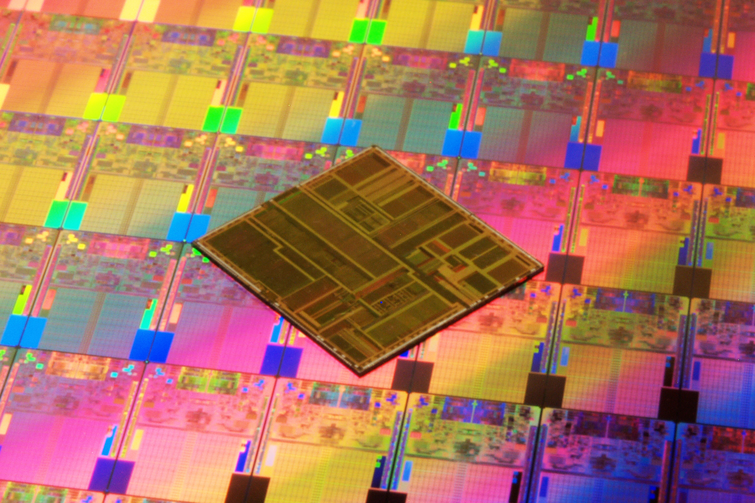
Mr. Krzanich did not reveal a lot of details about the company’s 10nm fabrication process and the exact reasons of the delay, but he implied that the new manufacturing technology uses FinFET transistors with enhancements and immersion lithography with a lot of multi-pattern steps.
“Each [process technology] has its own recipe of complexity and difficulty,” explained Mr. Krzanich, who once was responsible for manufacturing operations at Intel. “14nm to 10nm is the same thing that happened with 22nm to 14nm [transition]. The lithography is continuing to get more difficult as you try [to scale down]. The number of multi-pattern steps you have to do is increasing. This is the longest period of time without a lithography node change.”
The chief executive of Intel also implied that the company will not take any shortcuts just to get to 10nm in time. The new process will feature smaller transistor fin pitch, transistor gate pitch as well as interconnection pitch compared to 14nm technology in a bid to maximize transistor density.
“We believe if you take a look at the scaling, it will be quite strong relative to the normal scaling parameters that occur with the Moore's Law transition,” said the head of Intel. “I am not going give you the exact numbers right now. We think if you combine all those together, our leadership position [in the industry] does not change, even with this date.”
Intel said that while for now its manufacturing technology cadence is stretched to essentially 2.5 – 3 years, the company will try to go back to its two years cadence. Quite possibly, the return of the problematic “tick-tock” cadence will require a switch to extreme ultraviolet lithography. If the company’s 10nm process tech will be used to produce three product families (i.e., for three years), then EUV will likely become a viable option for 7nm sometimes in 2020.
It should be noted that stretching process technology cycles also mean stretching micro-architectural cycles. It remains to be seen how Intel will manage to improve performance from one processor generation to another and how significant performance improvements will be going forward.
Discuss on our Facebook page, HERE.
KitGuru Says: It looks like “Cannon Lake” processors have not been cancelled, but delayed by one year. If it is the case, then the rumoured “Ice Lake” chips may replace them in 2018, if Intel decides to stretch life-cycle of 10nm to three generations. Alternatively, “Ice Lake” may not emerge at all because using one micro-architecture for four years is not a good thing in general. Moreover, Intel may not need to use 10nm for three generations if EUV becomes viable by 2019.
“It remains to be seen how Intel will manage to improve performance
from one processor generation to another and how significant performance
improvements will be going forward.” –> The last few generations there was even almost no improvement already apart from iGPU. And that’s with node shrinks.
well i blame amd for all this, if they would not have gone with faildozer we would have a market with two competitors much more powerful products and not to mention true innovation, at this point intel has zero reason to compete with itself, it makes no sense so ofcourse they dont have and dont want to push performance more than 5-10% per gen, if zen fails hedt market is done for,it will be worse than now
they moving to Tick-Tack-Tock in short
I can see what your saying@58
.
☛☛☛☛☛http//GlobalNetMoneyWorld⚦com☚☚☚☚☚
Don’t forget the power efficiency for mobiles.
That’s what you get when there is no competition in x86 but immense pressure from arm products.
Intel’s failure is AMD’s fault. What a surprise.
It’s hardly an Intel failure when you consider how they’re competing against IBM and Oracle in the HPC arena. Scale-Up servers are still an area Intel doesn’t do so well in. Not to mention Intel is now moving into its coprocessor product line heavily the same way. And all those innovations used to fight there trickle down to the desktop and mobile chips. It’s not Intel’s fault software hasn’t kept up with newer instruction sets and multithreaded code is only just starting to come into play.
No, of course not, it’s AMD’s fault. Everything is AMD’s fault.
Yeah I know. I was thinking of performance improvements. Not performance/power improvement.
That’s not an AMD failure. That’s the failure of TSMC, GloFo, and Samsung. Although, truth is both Nvidia and AMD could have paid Intel/IBM to use their foundries and move to a lower node. High power is high power, and Intel was already making the Xeon Phi 650mm sq. dies on 22nm FF, so it’s not as though die size would have been an issue.
It was something in the tech world that didn’t go as planned, therefore it was AMD’s fault. C’mon, you know this.
No, it’s the fault of the foundries. AMD made lemonade and invested in HDL research to make up the difference in the meanwhile.
But obviously, if AMD had pulled a new CPU uarch out of thin air when they realized that Bulldozer was going to flop, then they’d be competitive, and magically, Intel would never have had problems with 10nm and wouldn’t have had to delay it and do Kaby Lake instead. Didn’t you read the OP’s comment? This is AMD’s fault, just like the foundries having trouble with 20nm was AMD’s fault, just like every other problem in the tech world is AMD’s fault.
If they’d just made Excavator the first go around, AMD would have been fine.
And no… The only AMD problems are AMD’s. The failures of other foundries and companies have nothing to do with AMD not delivering the proper Bulldozer or not providing a whole new lines of graphics cards with the 300 series (if they’d just upgraded all the GPU architectures to GCN 1.2 I think we’d have all been happy).
You’ve been spending too much time in the comments at wccftech if, after all this, you still think I’m being serious and not just pouring sarcasm over everything I’m writing.
I pretty much agree with all of your arguments. I’m mocking the guy who thinks Intel delaying 10nm due to production issues is somehow AMD’s fault for not being competitive.
I thought that was the running joke…
Ahh… on my end it felt less like you were playing along and more like you were actively trying to debate the point. My mistake if I misinterpreted that. 😆
daddas
What I find more surprising is how everyone expects Intel to just pull performance out of their a**. Like if AMD had competing product Intel would magically unleash a CPU with twice the IPC of SkyLake. The fact that they’ve managed 15% IPC improvement over Haswell is already a very decent achievement and certainly more exciting then Sandy>Ivy>Haswell>Broadwell transitions were.
Guess people still don’t understand just what Intel achieved with Sandy and why since then there’s no major improvement on Intel side of things in terms of raw IPC, not counting instruction sets who’s utilization is almost entirely up to software developers.
I won’t even talk about AMD since they still have major catching up to do before they’re anywhere close to “pushing performance further”, if they ever reach that point in CPU business again.