

Many sources from the GPU industry indicated last month that neither Advanced Micro Devices, nor Nvidia Corp. plan to make major GPU introductions at least till late in 2014, or maybe even early 2015. However, a Czech web-site this week not only revealed what it claims to be the specs of the GeForce GTX 880 graphics card and the GM104 chip, but also reported that Nvidia plans to introduce the new solution this summer.
Possible specs of the GM104 revealed
The GM104 graphics processing unit, which will succeed the almost legendary GK104 chip, is projected to feature whopping 3200 stream processors, 200 texture units and 40 raster operating units (a strange number!) as well as 256-bit memory controller. The GPU will consist of 7.9 billion of transistors and will be made using 20nm fabrication process, according to PCTuning web-site.
It is reported that graphics cards based on the GM104 will feature dual-slot cooling systems and will carry 2GB or 4GB of GDDR5 memory clocked at 7.40GHz. It is also expected that the graphics chip on the reference boards will operate at 900MHz clock-rate.
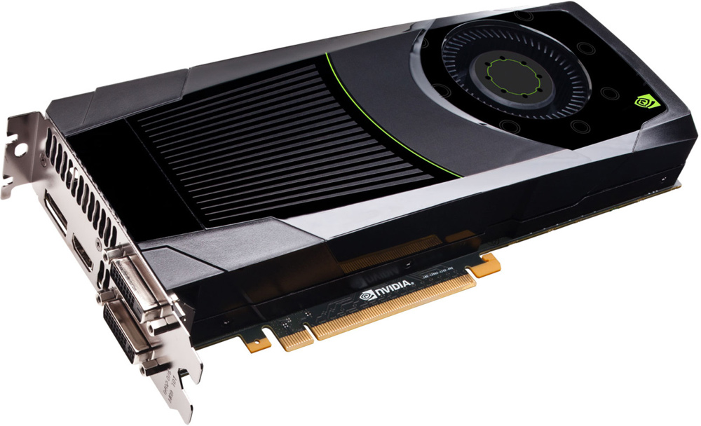
Nvidia GeForce GTX 680
It is interesting to note that the reference graphics card based on the GM104 is projected to sport only one 6-pin PCI Express power connector, which means that its maximum power consumption will be 150W (75W over PCIe slot and 75W over power cable).
Specifications of the GM104 GPU could not be confirmed with independent sources at press time, so we decided to analyse some of Nvidia’s past GPUs to figure out what the GM104 should be like.
Die sizes and transistor counts
Based on the specifications of different Nvidia chips released in the last five years, die sizes of the chips positioned for the same market segments remained similar:
- High-end: 529mm2 – 571mm2 (the GT200b is not a good example of a performance chip since this is a shrink of another GPU that was developed just to cut-down costs);
- Performance: 294mm2 – 332mm2 (the G92b is not a good example of a performance chip since it is also a die shrink);
- Mainstream: 221mm2 – 238mm2;
- Low-end: 116mm2 – 118mm2;
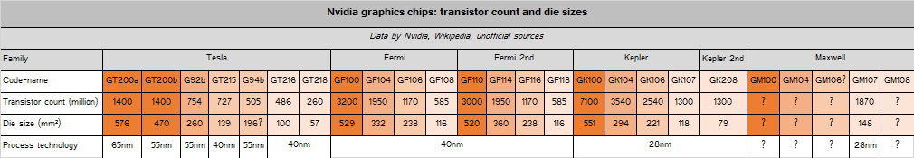
Architectures, process technologies and other things change over time, but die sizes of the chips remain on the same level. While there are exceptions, they just prove the overall “rule”. With that said, we can guess die sizes of the upcoming GPUs that belong to the Maxwell family.
Transistor count has consistently increased in accordance with the Moore’s law. In general, every new generation more than doubled the amount of transistors for the high-end chips, but that was not always true for performance, mainstream and low-end GPUs due to various reasons. While there is some kind of dependence of the transistor count of different GPUs within one family on the transistor count of the flagship chip, it is not really consistent across different GPU lines, so guesstimates regarding the Maxwell here can be absolutely wrong.
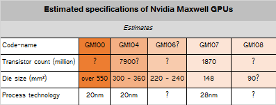
Still, what we do know is that a chip featuring 7.9 billion of transistors should be made using 20nm process technology in order to hit the same price-points as the GK104 did. It is also pretty logical to expect the flagship GM100/GM110 chip to be made using 20nm fabrication process. At the same time, it is possible that Nvidia could make GM106 chip using 28nm fabrication process to completely replace all the GK106-based solutions as well as graphics boards powered by cut-down versions of the GK104.
20nm: ready or not?
There are a lot of signs that Nvidia needs TSMC’s 20nm fabrication process to complete the Maxwell lineup and show a huge performance bump. Of course, there is also a possibility that Nvidia could just develop Maxwell-based GPUs while maintaining existing transistor counts and die sizes. This could give Nvidia GPUs a speed bump while retaining their current costs. However, this is generally an unlikely scenario.
Only recently it was reported that the yield of 20nm chips at TSMC was around 50%, which is too low, keeping in mind that nowadays the world’s largest maker of semiconductors charges its customers on per-wafer, not per chip basis. Hence, until the yield issues are solved, it does not make a lot of sense for Nvidia to make chips using the 20nm manufacturing technology.
Summing up
All-in-all, while it is possible that the GM104 (and GeForce GTX 880) will indeed be made using 20nm fabrication process, consist of 7.9 billion of transistors and contain 3200 stream processors (thus beating the GeForce GTX Titan Black in many applications), chances that it will be released this summer are pretty thin, unless there is a major development with yields at Taiwan Semiconductor Manufacturing Co.
Nvidia and TSMC did not comment on the news-story.
KitGuru Says: As it usually happens with the rumours, they can miss important pieces and the reality may turn out to be completely different than the logic tells us now.
it’s just a poster (pctunnig) desire in the first sentence says that it will be possible only under.
everyone from him his wish – Copy untruth.