

Nvidia Corp.’s new high-end graphics cards – GeForce GTX 980 – are expected to be introduced in several days from now, but a media report has already revealed what is claimed to be the final specifications of the new graphics boards. The specifications of the new Maxwell architecture-based flagship graphics solution are pretty surprising.
As it appears, Nvidia’s code-named GM204 graphics processing unit is considerably more powerful than initially thought. The GM204 integrates 5.2 billion transistors and features 398 square millimetre die size, which means that it will hardly be able to address mainstream market segments any time soon due to significant manufacturing costs.
Nvidia GM204 GPU in its maximum configuration packs as many 2048 stream processors (SPs), 128 texture units (TUs), 64 raster operations pipelines (ROPs), 2MB L2 cache, and 256-bit memory interface, according to a report from VideoCardz. The chip is organized in four graphics processing clusters (GPCs), each of which featuring four streaming multiprocessor modules (SMMs). Each Maxwell SMM sports its own PolyMorph Engine 2.0 unit (one vertex fetch, one tessellator, one viewport transform, one stream output, etc.) and is divided into four blocks with their own control logic (instruction buffer, warp scheduler, dispatch unit), a register file, two TUs and 32 SPs.
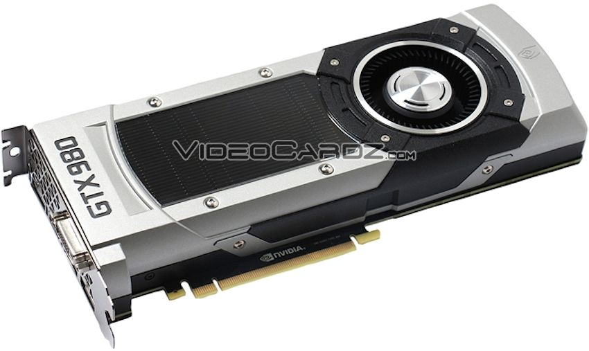
GeForce GTX 980 graphics cards made in accordance with Nvidia’s recommendations will feature 1126MHz/1216MHz base/boost clock-rate for GPU as well as 7GHz effective frequency for GDDR5 memory. The maximum single-precision floating point performance of the GTX 980 is projected to be around 4.6TFLOPS, which is significantly higher compared to that of the GK104-based GeForce GTX 770 (3.2TFLOPS), but is still lower compared to that of the GK110-powered GeForce GTX 780 Ti (5.1TFLOPS).
Thanks to 64 ROPs, the GeForce GTX 980 graphics card should perform very well in high resolutions. However, since its memory bandwidth will be limited to around 224GB/s it will hardly outperform the GeForce GTX 780 Ti or the GeForce GTX Titan Black in ultra-high-definition cases. Still, new colour compression technologies and other methods of reducing requirements for memory bandwidth could help to bring performance of the GM204-based solutions closer to that of GK110-powered graphics boards.
Nvidia did not comment on the news-story.
Discuss on our Facebook page, HERE.
KitGuru Says: Nvidia’s decision to boost the size of the GM204 GPU to nearly 400 square millimeters is very surprising. The manufacturing cost of such chip may be too high to use it for mainstream graphics products that cost around $200, meanwhile, at present the company still does not have a Maxwell-based mainstream GPU. The die size of the GM204 graphics chip may give a glimpse at what to expect from Nvidia when it comes to its new top-of-the-range GPU. It is highly likely that the code-named GM200 processor’s die size will be between 550 sq.mm and 600 sq. mm., which means that it will be the world’s largest GPU ever made.

So… The Ti and the 980 are different classes of cards. Why do you keep comparing them? 980 performance upgrade should be compared against the normal 780. When the 980ti releases, then compare them.
in what kind of way are the cards different (since they are in different classes as you say.. )
780- 780Ti ?
[Very serious Q… since they now jumped one Lvl ( 8xx) and upon that, mixed in in it all,
we have different Chips in so many and sometimes “same” cards…re-branded ?
that I have lost all controll over whats new… whats re-branded and if ” Really” a higher Hz regarding GPU /memory per definition is.. a “new ” card ?
… – confused.
In the simplest terms possible, the 780ti stock and unmodified is roughly 20% better than the 780 stock and unmodified. The progression goes 770 < 780 < 780ti. The new 900 series has newer architecture as well.
Does anybody remember this roadmap? – http://www.xbitlabs.com/images/news/2011-08/nvidia_kepler_maxwell_roadmap.jpg
Does anybody remember this roadmap? – http://www.xbitlabs.com/images/news/2011-08/nvidia_kepler_maxwell_roadmap.jpg
Why don’t you just list the spec. Reading the whole paragraph for spec isn’t worth IMO.
I think that is for CUDA performance and not for DX gaming performance.
They have basically met that goal.
If you notice the graph is in regards to performance per watt, Maxwell is roughly 45-50% more power efficient so the graph holds true.
For 499$ the given cooler with its backplate is of high quality. We should compare the gtx 980 with a stock gtx 780 to not with a oc’ed one. Also there is no need for a card that performs more than a gtx 780 ti, while consoles are still having a 7870 performance. No games will be optimized for PC. Good going Nvidia 180w for a card at this level is impressive.
consoles are not running on a 7870 more like a piece of shit
As simple as when the 980 Ti will come out, which will be the proper comparison card for it. The same goes for Titan, which is a whole different beast in market/performance/pricing. It’s just unnecessary to compare them. You don’t go around comparing a regular Intel i7 Processor with an Xeon E7, do you? For that matter, why not compare to the Quadro Series? Oh wait.
Good day.
PS4 may have a near 7870 performance. Xbox one 7790. I have listed official specs only
so confused so…
Sounds kinda dumb. Nvidia has only done one of their highest end cards with a Ti variant, and that was the 780. I highly doubt they’ll do a 980 Ti. Also who the shit cares. They are just names. Performance matters and thats the only thing that should matter. Yes you can compare a Xeon to an i7 extreme. The 5960X is very comparable to the Intel Xeon E5-2687W and many of the lower xeons are directly comparable. It’s as if Intel and Nvidia keep trying to get you to buy stuff that is 10% better and pay that high premium once again… Hmmm… Not very Moore’s like.. The 900 series is definitely one to be skipped.
No, the 780 Ti stock is less than 10% better than the 780. It’s around 5-7% I’d say.
Also the fps might be higher on the 780 Ti than the Titan or the Titan Black but if you look at the frame time variance, it’s more than double in most games. Now the applications of each are different for sure, as Titan and Titan Black were built for something else but I can guarantee they will feel smoother at 2160p than the 780 Ti just cause of the massive frame time variance on it. It only matters in higher resolutions really, but, honestly if you’re buying one of those cards for 1080p or 1440p, it’s really overkill… Considering you could get that 120-144fps/hz on a lower end card or even dialing down the settings a bit.
I kinda feel like the people on here are drones to Nvidia, AMD, and Intel… Such little performance gains and people go nuts and try to oversell it..
So according to you Nvidia should not release faster GPU’s for the next 6 years are so, because consoles have crappy performance?
But the graph shows a 300% improvement, not 45-50%?
Why compare those? They are not in the same price bracket?
The comparison to 780ti makes sense as it’s comparing the current top card to the new top card. (Ignoring the Titans of course, which are silly money). Why would you compare the 980 to the second best card currently widely available?
Considering the situation there is no need for that much performance, this is a nice time for them to concentrate on power efficiency. However they will go for a nominal increase in performance. The same card will be released in 20nm architecture which will increase performance and power efficiency further.
I really disagree here. We need a lot more GPU power to drive those 4K monitors that can be had for a reasonable price right now. Furthermore, if Nvidia would no longer develop really powerful GPU’s, they would become obsolete, since iGPU will be enough in a few years.
To think they wont release a 980 ti a few months after the 980 is absolutely ridiculous.
Single gpu cards cant even come close to maxing out framerates on a 120hz 1440p monitor, let alone 4k. Victor is stuck in 1080p land.
No 4k resolution is not for the majority. PC gaming itself is a dwarf compared to consoles. Myself like gaming in 4k. Hardly 5 to 10% of the pc gamers can afford that. Also always Nvidia waits for Amd to fireback and then they will release an updated model, just to keep that high performance crown. So this how they will go for the next 3 years, my guess.
No… The 780 ends up at around 3.97 tflops, while the ti is at 5.04. Given those numbers, it’s a ~25% increase in performance. I was being modest apparently. Using FPS as a measurement tool is not accurate. There are plenty of ways that much, much cheaper cards can match a 780 in fps.
Of course, if fps is the only thing that matters to you, then you wouldn’t be buying a 780/780ti.
http://www.pcper.com/reviews/Graphics-Cards/NVIDIA-GeForce-GTX-780-Ti-3GB-Review-Full-GK110-Crashes-Hawaii
Also, nobody is being a “drone”. It’s an nvidia article, so we are talking about Nvidia.
Thats what I was asking. Every article from KG has said “The 980 will not outperform the 780ti”, and I was asking “why compare them?”. It makes no sense.
Do you not understand how the technology advances? You aren’t paying for the X% increase in performance, you are paying for the newer tech. The 900 series is a completely different architecture than the 700 series.
You say the 900 series should be skipped, but you leave out that the 900 series uses Maxwell, which can save on power bills. Not to mention the cards haven’t been officially revealed yet. We don’t know what features they will come with. We don’t know what improvements they have software-wise. You are making these judgments on sites that are posting nothing but speculation.
“hey still have another year to double the performance of the Titan” – No they don’t. There is no time limit to double performance. There is no need to double performance. Hell the cards that are relevant to the article are more than what is needed for 95% of the PC gaming community.
I mean.. Serious question.. Do you have any idea what you are talking about? You seem like a person with “gamer knowledge”, and that’s fine, but your lines of reasoning are like 100% wrong.
4K is not yet mainstream, but this can change fast. Give it 1-2 years. And PC gaming is not a dwarf compared to consoles:
http://www.pcgamer.com/2014/09/12/there-are-711-million-pc-gamers-in-the-world-today-says-intel/
Now, you can take Intels numbers with a grain of salt, however remember Steam has a user base of around 75 million gamers. These are not small numbers.
ti stands for titanium there a very little in difference between the two maybe more shaders and a faster clock speed http://www.evga.com/articles/00694/#3662 http://www.evga.com/products/product.aspx?pn=02g-p4-2662-kr
(A-hem) …880… (cough, cough) 😛
Whoops, I incorrectly referenced the article. Google maxwell performance per watt, according to Nvidia’s press release in February Maxwell has twice the performance and 50% less power consumption, which held true with the 780 TI based in maxwell. So they would be right on target with the graphs. *edited for crappy spelling due to phone.
There wont be a 980ti unless AMD’s 390x has serious performance, and from the sound of it, it will be a good card, however i am hoping Nvidia can put their heads together and start releasing proper power cards, not just make do cards,- i.e we will give you a card that is just a little better than the last but not by a lot, and i am talking the difference from the 980 to the std 780.
Because each generation was faster than the last. There is no actual need for a new generation if it brings no tangible benefits, and given how GPU limited almost every application that uses real time graphics (mostly games) are, then having more GPU power is almost never enough.
If indeed this generation is less fast than the previous one it would be a first in a 20 years of GPU history, it would set a bad precedent that will greatly harm the consumer and eventually the industry as well (an industry that ceases to innovate, or slows considerably their evolution cycles is eventually outshined).
GTX 780 was faster than GTX 680 which was faster than GTX 580, which was faster than GTX 480, which was faster than GTX 285 (the equivalent of a TI card BTW), which in turn was faster than 9800GTX, which was faster than 8800 ULTRA (another TI equivalent).
See the trend? Never before a new gen was slower from *any* single GPU of the last genereation. I seriously hope that GTX 980 won’t be “an unfortunate first”.
Here is what you are missing. I’m going to quote them again. “The 980 will not outperform the 780ti”. One more time: “The 980 will not outperform the 780 TI”. The 780TI is a bracket above the 980. There is no reason to compare them. The 980 already outperforms the 780.
Is that a quote coming from an official source?
Because if so it makes little sense, both the price that the card is set to be released, the leaked benchmarks and leaked specs show about a 10% lead.
Which also makes sense historically, nVidia ‘ s “next gen” mid end (what GM204 really is) about matches or slightly supersedes last gen’s high end (gk110) and that’s true in most chips generations of theirs.
The labels communicate where the card sits in the series.
Each successive generation of X80 outperforms the last X80, just as each X70 outperforms the last X70 but not the X80 of its own series.
The X80 Ti cards are a step above X80. See the 650 and 550 Ti as an example. The former did not outperform the latter, because it was one series up and did not occupy an equivalent position in its series.
Its in this article we are commenting on. “4.6TFLOPS, which is significantly higher compared to that of the GK104-based GeForce GTX 770 (3.2TFLOPS), but is still lower compared to that of the GK110-powered GeForce GTX 780 Ti (5.1TFLOPS).”, in this other Kitguru article http://www.kitguru.net/components/graphic-cards/anton-shilov/nvidias-geforce-gtx-980-will-not-beat-geforce-gtx-780-ti-insider/ and also in most articles on it over the internet. I’ll post a few under this. The comparison I’ve seen the least is 980 vs 780, and it baffles me.
http://www.kdramastars.com/articles/37780/20140916/gtx-980-vs-gtx-780-ti.htm
http://www.digitaltrends.com/computing/nvidia-geforce-gtx-980-specs-allegedly-leak-days-reveal/
And many more. This last one makes sense though.
http://wccftech.com/nvidia-geforce-gtx-980-replace-gtx-780-gtx-780-ti-custom-980s-8gb-vram/
haha… they wont call it Ti…they will call it Tx…. so then your wrong anyhow.. ha ha..
😉 😉
As far as gaming performance goes GM204 based cards seem to be faster. As far as Raw-folding power then GK110 clearly wins. So it’s a matter of perspective I guess (on which one is faster and on which one is not). Even that -though- tracks with nVidia’s past releases, GK104 (mid-end chip, actually) was slower than GF110 (previous gen’s high end) in folding power yet faster in games. We get a repeat of that, only -this time around- due to the node shrink not being ready in time the differences (in gaming power) are not as significant as it was between GF110 and GK104.
Still it’s impressive what a new architecture can do, on the same node no less (2/3rds less TDP for the same gaming performance).
More operations does not equal more performance.
Efficiency is essential. If you have a card that can do 8 tflops but another card can only do 2 tflops.. but the latter can do the same tasks using 1/8 the cycle of the former, then it’ll wreck it.
I think you need to study how computing works in the first place….. I bet you think overclocking an i5 or water cooling a lower end gpu is brilliant instead of buying the higher up. I mean the i5’s have very similar specifications as an i7, so OC should make them even yeah? I mean how come OC only boosts your performance so minimally? Hmmm. Must be just random coincidence.
I didn’t just say Nvidia. I said AMD and Intel too. Fork over that $700 for that brand new part that performs 10% better. Good on you. Show ’em who’s a true consumer.
Did you really bring power bills into this? Honestly, you’re challenged just on that statement alone. Considering you could go with a 285 or 770 and not upgrade and still have that extra couple hundred bucks to save on power. You sir, are stupid.
Paying $700 for “new” tech that doesn’t perform 50% better than last gen is going against how technology is supposed to work. Every two years doubling of performance is supposed to happen. New software.. Yup, go ahead and buy that new item that has that new software, pay that premium for those little gains.
Ignore Moore’s law. Be okay with the crappy things they feed you. Think they are gold. Be the consumer you were born to be.
I’ll be waiting for real improvements to come out. Not garbage rehash and minimal gains. It’s worthless. No, I’m not a gamer, I’m a computer engineer. I do game but thats not the point at hand. The point is that performance is essential. It is the key part. We still lack efficient hardware. You can talk about software all you want, it’s the efficiency of the cycles that matters the most. We still have to use so many cycles to get one task done, they’ve even fallen behind to just milk people for their money rather than innovate. It’s disgusting and I wish to create products that actual do innovate and are worth those upgrades.
No… This is completely wrong.
“Honestly, you’re challenged just on that statement alone.” – No I didn’t, but that was clearly the only statement you understood.
“Paying $700 for “new” tech that doesn’t perform 50% better than last gen is going against how technology is supposed to work” – No it isn’t. Obviously you haven’t ever paid attention to any other technological field in existence. Solar cell researchers celebrate the ability to go from 18.5% efficient cells to 20.5% efficient cells, and their price jumps by the thousands. Nuclear Fusion was happy to get a <1% efficiency increase to put their power generation in the positive section. In tech, ANY improvement is progress, since improvement is not able to be increased at a set increment, especially when dealing with new architecture that can be improved through software.
"pay that premium for those little gains." – Again, look at how tech works. You clearly don't know.
"Ignore Moore's law" – Again, lack of education: http://www.researchgate.net/publication/222660481_End_of_Moore's_law_thermal_(noise)_death_of_integration_in_micro_and_nano_electronics/links/00b4952c445214363e000000
"I'll be waiting for real improvements to come out. Not garbage rehash and minimal gains" – Not sure why you keep saying its a rehash, since its literally a 100% different chip. Proving your lack of knowledge again.
"I'm a computer engineer" – No you aren't. Your posts prove that well enough.
"The point is that performance is essential." – Yes it is, but performance is a lot more than FPS increase. Do you even know how TFLOPS are measured?
Your whole rant about cycles makes no sense, since there is no set class of task which require a set number of cycles. There is no measurement for it. The number of cycles required is different for every task.
"It's disgusting and I wish to create products that actual do innovate and are worth those upgrades." – I guess you don't buy ANY hardware then, since Nvidia and Intel are the only companies with dedicated research departments to advance the hardware. AMD just adds more cores and leaves out tech to keep their budget niche.
Anything else? You have a huge misunderstanding on how technological advances work. You feel entitled to a 50% increase for some reason, and that baffles me. You are basing your argument to complain about a card that is 1) WAY too powerful to begin with for 90% of applications, and 2) "only" 20% more powerful on a more efficient architecture that has 100X more potential than our current hardware. Its #2 that keeps throwing you for a loop. Maybe you can try to understand.
Look up IBM. They have carbon nanotube based chips and a new racetrack drive coming. They learned from their mistakes and not to feed off just 1 architecture. Even still, google is spending tons in quantum computing and many other companies are developing new chips. x86 and x64 will be silicons last, and its death. Intel and AMD will die unless they can adapt. Its how technology works. You don’t adapt quick enough then something else comes along to destroy you. They aren’t following Moore’s law with silicon, hence something else will come to ruin them. It’s how it works. Moore’s law isn’t exact every 2 two years, as new innovations must come to change that. Moore’s law is not your standard “law”, it’s something to abide by rather than something that must be followed. So deviants may come along, like Intel and AMD, and they may hoard away one architecture (they hold that license exclusively really). So they aren’t trying to push forward, they are trying to hold back, in the long run anyway. Other companies will innovate around them to make those increases. Hence, Moore’s law will return.
The death of silicon is coming and it will come sooner than you think.
You can’t relate solar to this. Why don’t you just bring Barney and friends into the discussion as well yeah? It may be an improvement but the use and cost of that item is what matters, which is the point I was making. The extra electricity bill does not equate for a brand new $700 card. You can’t even read.
Wow AMD hater huh? Well, they advanced hardware to be more compatible at 4k resolutions.. Hence those tflops were more efficient at that level. It wasn’t that great, but they proved the efficiency. Building parts to be efficient at one task is what we are at right now, and its minimal. I don’t think you understand how cycles work. They are exactly that, cycles. If you don’t understand what cycle means, then you’re even dumber than I thought.
I don’t think you understand how it works at all. You just spout information like you are some tech genius. You aren’t. You’re a regular user trying act like he knows what he’s talking about. Exactly why you said “90% applications” won’t use them. Almost everyone in the industry, media, modelling, architecture, engineering, servers, and so much more need those 50% boosts every year, or at least doubling of performance every 2 years.
You are holding back the industry. You promoting Nvidia, Intel, and AMD. You are holding it back. I get that you can use it and it is applicable, cause it does work, but they are bleeding cash out of everyone for minimal gains. No real innovation or true jump has come along for 8-10 years.
They will die. No matter how long you hold onto, they will die out because of their current actions.
You can shut up and go take some classes and learn from people who actual innovate now.
Wow.. So much nonsense.. You aren’t even worth replying to. The only thing you’re right about is the death of silicon, but its not as close as you think.
Quantum computing isn’t replacing processors any time soon. The only chip in the pipe right now is the Vesuvius 512 qubit chip, and its performance has been extremely erratic and unreliable. Sometimes being outperformed by two Xeon chips, and sometime being faster than seven. Its not replacing anything anytime soon.
If you don’t think Intel or Nvidia have a plan or is researching quantum, then you are nothing short of a complete moron. They are probably being smart and waiting for a stable quantum architecture to work off of before investing. AMD was sure would die off anyway, seeing as their big counter to the titan was to strap two 290X chips on one board and brag, even though the titan is for a 100% different purpose.
Why isn’t solar comparable to this? They are looking in performance increase just as GPUs are. They are very comparable. You just don’t like it because it shoots down your point. Nobody said you HAD to upgrade your gpu. Most would recommend upgrading every two years anyway, and that generally brings two generations. All I was saying that it was a BIG improvement. Maxwell is what knocked out the AMD mining control. Efficiency is huge. You seem incapable of understanding that.
“Well, they advanced hardware to be more compatible at 4k resolutions” – You mean they copied Gsync and added Displayport support. Good job. Every single review on the internet, minus the obvious bias ones, puts Nvidia ahead in 4k performance.
“I don’t think you understand how cycles work.” – I don’t think you understand how using cycles as a measurment of performance is 100% irrelevant and inaccurate, since cycles are ambiguous. Your explanation of them is terrible.
“Exactly why you said “90% applications” won’t use them” – Wrong. The only applications that come close to maxing out something like a 780ti would be a rendering program like the Autodesk suite. The percentage of people buying a 780ti for autodesk is more than likely <10%, seeing as dual chip cards are better for it. Failing that, you can get two cheaper cards and get better performance in Autodesk than a single gaming card, since those are calculation based.
"You are holding back the industry" – No, uninformed people such as yourself asking for unreasonable or downright magic advances in technology hold the industry back. You act like releasing this card is the end of all research, and we should demand more. Its just stupid. I've not ever seen such an illogical argument before. The reason the price is so high is because part of the cost goes directly to research and development.
"so much more need those 50% boosts every year" – No they don't, since software is build around hardware. Autodesk won't make a program that needs 128GB RAM because no computers would run it. They make software based on the hardware available. Not to mention in pretty much all of those fields we can make any object imaginable. If you can't model something with 2,000,000 polys then you are a very inefficient modeler.
You keep blabbing about quantum. Do you know how much a quantum processor costs to make, let alone sell commercially for profit? There is a reason only the two top companies in their fields have one, yes One. They cost more than both yours and my salary combined for the next 10 years. Have you seen what they look like? They look hideous and are completely impractical since they are in very, very early prototype stage and are completely erratic in performance. We won't see quantum reach consumers until at least 2025 area. At the earliest I'd say 2020.
You are rushing what is currently more than 80% in the realm of science fiction. I understand that its cool, but we have this nice thing called "reality" holding us back. Its just stupid to demand a 50% increase in performance. We should be looking for efficiency as well as power, especially at a time when a majority of our uses don't come close to maxing anything.
You still can’t read. I’m not gonna reply after this.
Yes, thank you for agreeing. I said cycles mean nothing. Thanks for agreeing. Stop being a moron and denying it still. You grasp the concept but lack the implementation of the concept. The R9 290X was for gaming at 4k and the 780Ti and Titan Black beat it by such minimal stats for $200 or more. The 290X was a niche product for a niche application, and it worked. While they didn’t innovate really, they did help to promote adoption of 4K at cheaper prices. You can build a full 4k gaming rig with monitor for under $1500 with their gpu. When has Nvidia ever done that? I can’t think of one time.
No one should upgrade for electrical bills unless they are a new buyer. Most of the people who can afford this gpu are not gonna be a new buyer. Nor should anyone even still running the 500 series cards should upgrade to it. It’s a worthless product and they should’ve at least developed something worth buying. They just know how to bleed everyone for their cash.. Depressing that people still fall for it so damn much..
I said Quantum as another solution. They already have the D-Wave… but carbon nanotubes are what I’m interested in as its more tangible right now and has been for 20 years, just no one has put money towards it. No Intel and Nvidia are not working towards that. Intel is working towards Skylake, Broadwell, and 14nm process chips too. How moronic that you don’t even know what companies are putting their money towards. They both have stocks you know, people know everything they are working on, as they want to build up that stock and give their people an idea of whats to come. The consumers and the shareholders are being moronic right now and not promoting the future.
You’re an idiot. Have fun help ruin the industry. You can be the consumer you always wanted to be! The slave to minimal gains… Damn, you must be pulling all the women and have a nuclear reactor.