

Taiwan Semiconductor Manufacturing Co. has clarified the timeframe when it intends to start mass production of chips using 16nm FinFET fabrication process. The world’s largest contract maker of semiconductors once again will delay 16nm FF volume production by a month or two to the third quarter of 2015.
Back in October, 2014, TSMC already said that it would move mass production of chips using its 16nm FinFET manufacturing technology from early 2015 to Q2 or early Q3 2015. This week the company said that the aforementioned semiconductors will be made only sometimes in the third quarter of the year, which essentially means another delay, albeit, a slight one.
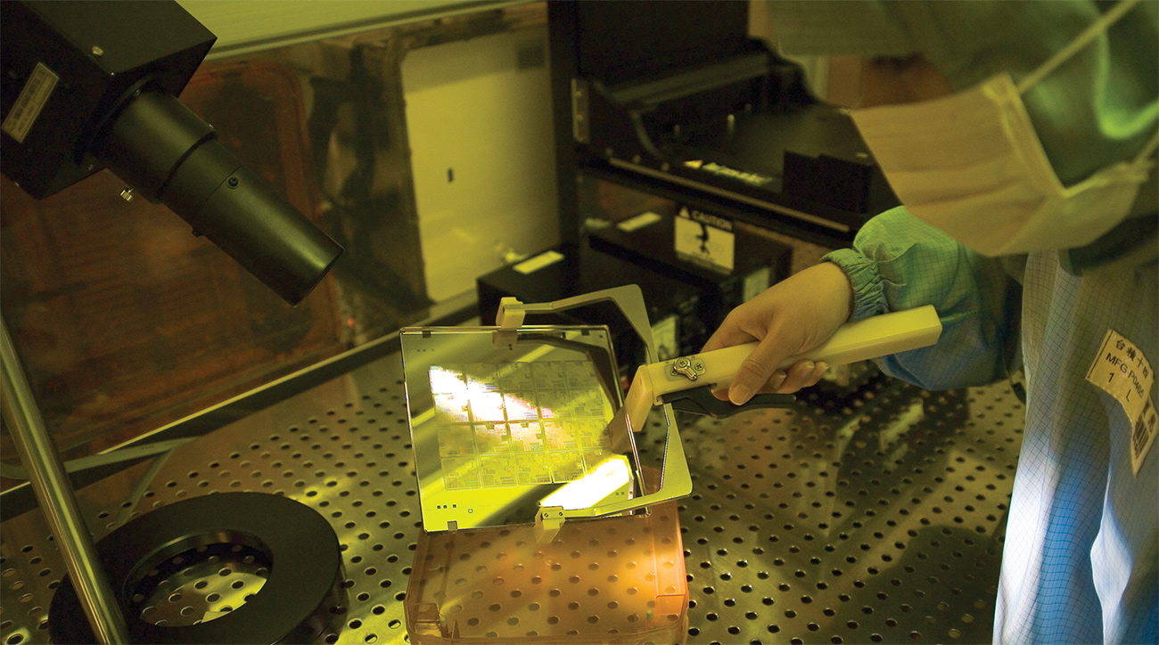
“We plan to mass produce 16nm FinFET [chips] in the third quarter of 2015,” said Lora Ho, senior vice president and chief financial officer of TSMC.
It will take the company around seven quarters to bring profit margins it receives from 16nm FinFET manufacturing to corporate average levels, according to the CFO. This year the company plans to produce 50 chip designs using the 16nm FinFET fabrication process.
TSMC’s 16nm FinFET (CLN16FF)and 16nm FinFET+ (which TSMC officially calls 16nm FinFET Plus) process technologies rely on the back-end-of-line (BEOL) interconnect flow of the company’s 20nm SOC (CLN20SOC) fabrication process, but use FinFET transistors instead of planar transistors. This provides additional performance and/or power savings, but this does not allow to significantly shrink the size of chips compared to chips made using the 20nm SOC. The proven BEOL interconnect flow means that it should be easier for TSMC to start mass production of chips using its 16FF and 16FF+ manufacturing technologies.
It is unclear how delay of mass production using 16nm FinFET process technology affects schedules of the 16nm FinFET+.
TSMC expects the capital expenditures for 2015 to be between $11.5 billion and $12 billion. 80 per cent of the company’s CapEx will be spent on development of 10nm and thinner manufacturing technologies, tools necessary to make chips using 16nm and 20nm fabrication processes as well as on other leading-edge technologies-related things.
Discuss on our Facebook page, HERE.
KitGuru Says: The situation with FinFET process technologies in general remains blurry. It is unclear when GlobalFoundries plans to start production chips using 14nm FinFET process it licensed from Samsung. Moreover, the volumes of 14nm FinFET chip wafers processed at Samsung are a complete mystery.