
Nvidia Corp. on Tuesday publicly updated its graphics processing units roadmap for the coming years. The company removed its code-named Volta architecture from the plan and introduced Pascal architecture instead. The latter is believed to feature similar innovations to Volta, but to be even more significantly tailored for low power consumption and will sport certain interconnection technologies not available today.
Named for 17th century French mathematician Blaise Pascal, Nvidia’s next-generation family of GPUs will include three key new features: stacked DRAM, a key innovation that was promised for the Volta family of GPUs; unified memory technology that is currently only available on AMD’s accelerated processing units (APUs) with heterogeneous system architecture (HSA) capabilities (e.g., Kaveri), and NVLink, a high-speed interconnect for graphics processing units and central processing units. When graphics processing capabilities are concerned, Pascal will support DirectX 12 capabilities.
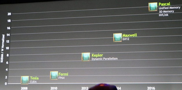
Nvidia roadmap. Image by LegitReviews
The stacked DRAM seems to become a key feature of next-generation GPUs due in 2016 and beyond from both AMD and Nvidia. Stacked DRAM allows to increase memory bandwidth and capacity without extending footprint or complexities of graphics cards. At present Nvidia expects two – four times increase of memory bandwidth and size with Pascal, but in reality there could be a much more significant boost. Recently announced HMC 2.0 devices (hybrid memory cubes, stacked DRAM devices designed by Micron and allies) have bandwidth of 480GB/s over 16-lane links. Four of such cubes could provide slightly south than 2TB/s of bandwidth.
The unified memory allows the CPU to access the GPU’s memory, and the GPU to access the CPU’s memory, so developers do not have to allocate resources between the two. Originally, this was a part of Maxwell architecture, but it looks like Nvidia removed the feature from the new family of chips. Keeping in mind that unification of memory requires collaboration between GPU and CPU designers, Nvidia’s technology is either a result of work with Intel and AMD (or just Intel), or there is a standard for CPU-GPU unified memory is incoming.
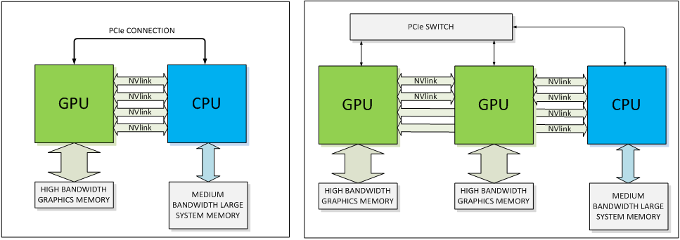
Examples of NVLink implementation
The NVLink is pipe between GPUs and CPU, which has total bandwidth of 80GB/s. Given the bandwidth that hybrid memory devices provide, there is a clear need for such an interconnection in a couple of years from now. NVLink is claimed to be twice more energy-efficient than standard PCI Express 3.0. The developer states that in an NVLink-enabled system, CPU-initiated transactions such as control and configuration are still directed over a PCIe connection, while any GPU-initiated transactions use NVLink. This allows us to preserve the PCIe programming model while presenting a huge upside in connection bandwidth. Moreover, when connected to a CPU that does not support NVLink, the interconnect can be wholly devoted to peer GPU-to-GPU connections enabling previously unavailable opportunities for GPU clustering.
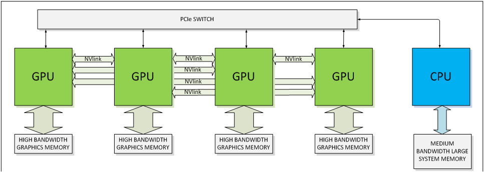
An examples of NVLink implementation
The Santa Clara, California-based GPU developer has been designing its high-speed interconnect for GPUs and its general-purpose ARM-based cores with supercomputers in mind for several years now. Perhaps, NVLink is the first fruit of this work. However, Nvidia will need to ensure that its NVLink is compatible with Intel, AMD, IBM and other microprocessors to make it an industrial solution.
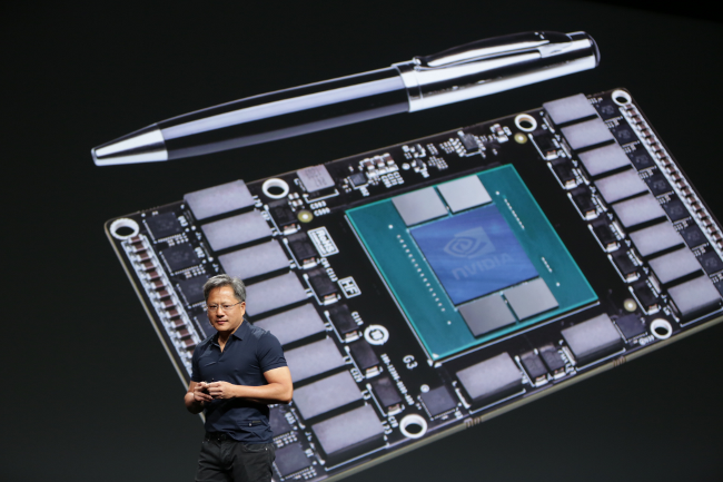
To demonstrate what Pascal architecture is capable of, Nvidia showed off its Pascal module, a device akin to an MXM module that holds a high-performance GPU with on-package memory.
KitGuru Says: Like all things that are two years off, Pascal looks very promising and capable. However, it is so far away that we do not know what software it will run and what challenges will face. For example, with massive bandwidth of hybrid memory devices it should be an awesome solution for 4K gaming. But by the time it hits the market, the latter will become almost mainstream.