
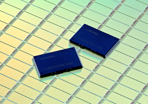
Toshiba Corp. and SanDisk Corp. on Wednesday said that they would start to produce multi-level cell (MLC) NAND flash memory using 15nm fabrication process later in April. The new manufacturing technology allows Toshiba to make world’s smallest and potentially cost-efficient 128Gb NAND flash memory.
Initially, Toshiba and SanDisk will produce 128Gb MLC (two-bits-per-cell) MLC NAND flash memory using the 15nm process technology at Fab 5 phase one, where the fabrication tech will replace the companies’ second-gen 19nm manufacturing process. The phase stage of Fab 5 is currently under construction, and the new technology will also be deployed there.
The new 128Gb MLC NAND flash chips achieve the same write speed as chips formed with second generation 19nm process technology, but boost the data transfer rate to 533Mb/s, 30 per cent faster, by employing a higher speed interface.
Toshiba claims that it had achieved the world's smallest class chip size with the 15nm process and improved peripheral circuitry technology.
According to SanDisk, the 15nm technology uses numerous progressive process innovations and cell-design solutions to scale the chips along both axes. SanDisk's All-Bit-Line (ABL) architecture, which contains proprietary programming algorithms and multi-level data storage management schemes, has been implemented in the 1Z technology to deliver NAND flash solutions with no sacrifice in memory performance or reliability. SanDisk’s 1Z technology will be utilized across its broad range of solutions, from removable cards to enterprise SSDs.
Separately, Toshiba announced that it would use the 15nm fabrication process to produce triple-level-cell (TLC, three-bits-per-cell, 3bpc) NAND flash memory. Such memory, provided that the yields are sufficient, will be the world’s most cost-efficient NAND flash. The company aims to start mass production of TLC NAND using 15nm process in June, 2014.
The company intends to develop controllers for 3bpc embedded NAND flash memory in parallel and introduce TLC NAND products for smartphones and tablets. Eventually Toshiba will use 15nm TLC NAND with special controllers for solid-state drives.
Toshiba and SanDisk run joint NAND flash manufacturing operations in Japan.
Discuss on our Facebook page, HERE.
KitGuru Says: If Toshiba and SanDisk manage to sustain 3000 write/erase cycles with 15nm MLC NAND (typical amount of cycles sustained by modern MLC), then the new memory type will enable lower-cost SSDs already this year. In case the new type of memory (like 15nm TLC NAND) requires new controllers, then its adoption will take time.