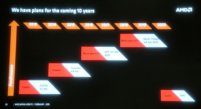
Advanced Micro Devices has been mulling accelerated processing unit for high-performance computing applications for many years, but software and hardware limitations have prevented the company from creating such chip. Recently AMD finally unveiled plans to release an APU for HPC market in 2017 and this week the first concept of such product leaked.
At present supercomputers use nodes featuring traditional multi-core x86 microprocessors as well as highly-parallel compute accelerators/co-processors powered by many-core architectures, such as Nvidia Tesla, Intel Xeon Phi or AMD FirePro. While such configuration of nodes generally works very well today, performance of many operations is slowed down by limited bandwidth between CPU and accelerators. For example, many applications could benefit from uniform memory access by CPUs and accelerators/co-processors as well as from cache coherency, but bandwidth and latency limitations usually slow things down. In a bid to solve the problem, Nvidia proposes to use high-bandwidth NVLink technology to connect CPUs and Tesla accelerators, whereas AMD intends to integrate CPU and GPU cores in the same piece of silicon in a way that allows compute engines to communicate efficiently with each other.
AMD’s accelerated processing units – which integrate x86 general-purpose cores and GCN graphics processing cores – available today are fine for consumer PCs, but for HPC applications a different level of integration is required. Not only bandwidth between x86 and GCN cores has to be increased and cache coherency maintained, but different processing engines have to efficiently and collaboratively use memory controller in order to realize all benefits of unified memory access. At present AMD is working on such accelerated processing units due to be available later this decade.
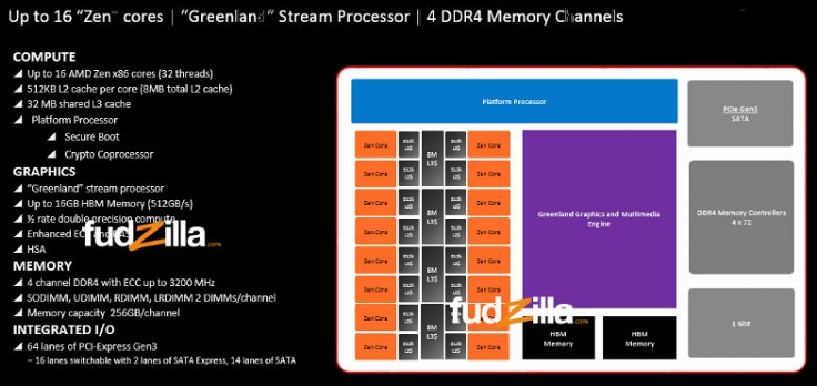
Fudzilla this week published an image that resembles slides from AMD’s documents for partners. The image describes an unknown APU without a code-name, which can be a concept of AMD’s upcoming accelerated processing unit for high-performance computing applications.
Expected to be released in 2017, AMD’s APU for supercomputers is projected to integrate 16 x86 “Zen” cores with two-way simultaneous multi-threading technology and 512KB L2 cache per core, 32MB L3 cache as well as a new-generation “Greenland” graphics engine with ½ double precision compute rate. The chip will also feature a quad-channel DDR4 memory controller with enhanced ECC capabilities that supports up to 256GB of memory per channel, 64 lanes of PCI Express 3.0 that can be used for SATA Express, integrated SATA, 1GbE, USB as well as various legacy interfaces. To further speed-up bandwidth demanding applications, the APU is expected to feature on-package 16GB of HBM2 memory with 512GB/s or higher bandwidth. Given that the chip is scheduled to arrive in 2017, expect it to be made using 14nm FinFET (14LPP) or 10nm FinFET process technologies.
Since the APU described in the slide does not have a code-name, release timeframe or targeted process technology and thermal design power, it is highly likely that the chip is a concept of what AMD might develop for various market segments.

For example, HPC would benefit from 16 x86 “Zen” cores, L3 cache, full-speed DP rate (which is ½ of single precision rate in case of contemporary FirePro accelerators), HBM memory and quad-channel DDR4 with ECC. At the same time, HPC applications do not need secure boot or crypto processors, SO-DIMM or SATA Express support. By contrast, consumer-class APUs do not need 16 x86 “Zen” cores (client PC programs are not optimized for multi-core/many-core processors, hence, 16 cores will provide 10 – 15 per cent performance boost compared to four cores in real-world apps), full-speed DP rate, large L3 cache, ECC with enhancements, 256GB of memory per channel and so on. However, consumer hybrid processors need enhanced security, flexible PCI Express configuration, support for different memory module types, legacy interfaces and so on.
AMD did not comment on the news-story.
Discuss on our Facebook page, HERE.
KitGuru Says: While it will be possible to design and build the APU described above using 10nm process technology, it is really unlikely that the chip will ever see the light of day in its current configuration. Therefore, consider the story not as the first details about an unknown accelerated processing unit from Advanced Micro Devices, but as a description of what AMD might plan to create in a couple of years’ time.
 KitGuru KitGuru.net – Tech News | Hardware News | Hardware Reviews | IOS | Mobile | Gaming | Graphics Cards


Just make it on time AMD (Another Manufacturing Delay)…… its humble request
►►►I RECEIVED FIRST DRAFT OF $13000!@ak11:
,
➨➨➨➨https://WorkOnlineBots.com/sets/position…
★★★★★★★★★★★★★★★★★★★★★★★★★★★★★★★★★★★★★
fhfg . I see what you mean… Clarence `s blurb is terrific, on friday I bought a great new Dodge after having made $4460 this past 4 weeks and-just over, 10k this past month . without a doubt its the most-comfortable work Ive had .
I started this seven months/ago and almost straight away began to bring home at least $70, per/hr . over at this website HERE’S MORE DETAIL