Two employees of Advanced Micro Devices have revealed in their LinkedIn profiles that they had worked on AMD Radeon R9 380X graphics processing units with vertically-stacked high bandwidth memory (HBM). The engineers at AMD essentially confirmed that the company’s next-generation flagship graphics processor will use HBM memory and will carry the “R9 380X” model number.
Linglan Zhang, a principal member of technical staff at AMD, wrote in his profile at LinkedIn that he was involved in development of the “world’s first 300W 2.5D discrete GPU SOC using stacked die high bandwidth memory and silicon interposer.” The engineer also revealed that the Radeon R9 380X is the “largest in ‘King of the hill’ line of products.” Previously it was believed that this year’s flagship GPU from AMD carries the “R9 390X” model number. The employee of AMD has already deleted the information regarding the next-generation AMD Radeon.
Ilana Shternshain, ASIC physical design engineer from AMD, also revealed in her profile that she was responsible for “taping out state of the art products like Intel Pentium processor with MMX technology and AMD R9 290X and 380X GPUs.”
Previously it was reported that AMD’s next-generation flagship graphics solution would feature HBM DRAM. Back in Q4 2014 SK Hynix even revealed that it would start mass production of HBM memory in the first quarter of this year.
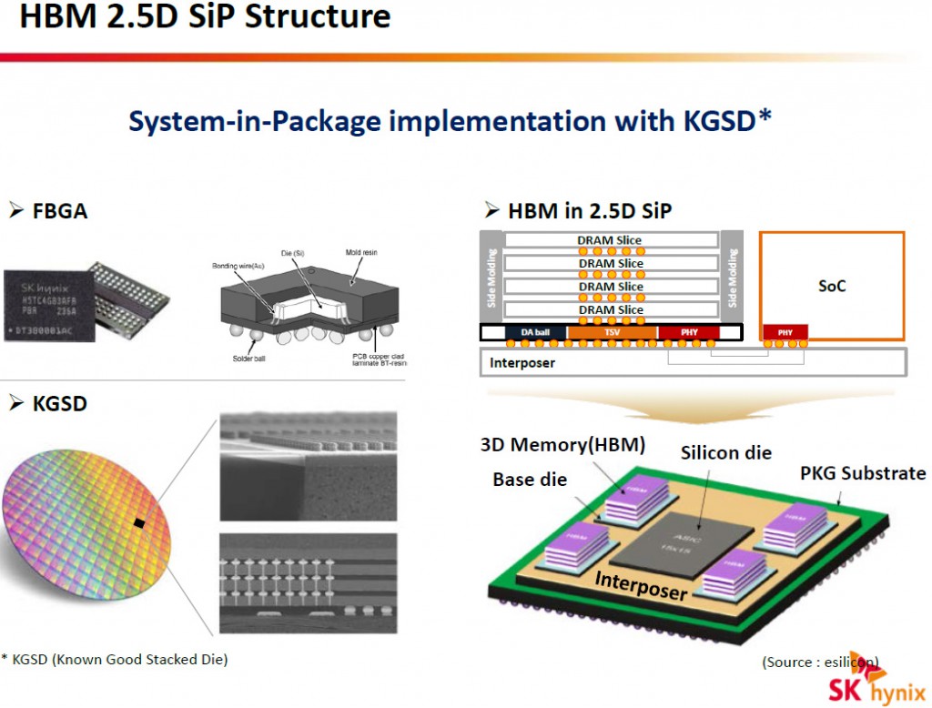
Each HBM IC [integrated circuit] stacks four DRAM dies with two 128-bit channels per die on a base logic die, which results into a memory device with a 1024-bit interface. Each channel is similar to a standard DDR interface, but is completely independent and therefore each channel within one stack and even within one die can operate at different frequency, feature different timings and so on. Each HBM 4Hi stack (4 high stack) package can provide 1GB – 32GB capacity and 128GB/s – 256GB/s memory bandwidth. The high-bandwidth memory chip uses 5mKGSD (molded known good stacked die) packaging that stacks four 2Gb dynamic random access memory dies on one base logic die.
AMD’s next-generation high-end Radeon R9 graphics processing unit is expected to feature 4096 stream processors/64 compute units, 256 texture units as well as 4096-bit memory interface to connect to four SK Hynix HBM devices. The GPU’s memory interface operates at 1.25Gb/s data-rate (1.25GHz effective DDR frequency) and delivers whopping 640GB/s memory bandwidth.
The LinkedIn findings were made by members of Beyond3D forums.
Discuss on our Facebook page, HERE.
KitGuru Says: It is interesting that AMD decided to use “R9 380X” model number for its flagship graphics solution. When AMD introduced its Radeon R9 200-series lineup, it rebranded older products to make the family complete; as a result, the Radeon HD 7970 became the Radeon R9 280X. If the new family's flagship carries the “R9 380X” model number, then it means that the Radeon R9 290X solution will not be renamed to something like the Radeon R9 380X. Potentially it means that AMD’s new GPU lineup will include a number of all-new chips and will not feature any re-branded products.
 KitGuru KitGuru.net – Tech News | Hardware News | Hardware Reviews | IOS | Mobile | Gaming | Graphics Cards


That bandwidth bro…
Sadly the power consumption does not seem appealing (through the info we have had till now). For 4K, this will be a beast; but for casuals and for 1080 people, NVidia will be a much better and reliable bet for 2015.
Surely this is the beginning of 4K
Fucking awesome!!!!!!
Seriouslee, the power consumption is something that we don’t need to care about. AMD is like: “How much your PS gives you? 1000W? Oke, we take it all to make you a really beast!”
300W seems like a lot, considering the 290X was only 250W at least anyway, but if you then consider that its gained over 1k in shaders AND a ridiculous memory system… this could be just like the 7970 in its heyday…
( 7970 on release had trumped any of the existing cards and even matched the dual-GPU cards at the time while being almost twice as efficient, 380X looks like it could do the same thing… )
and a lot of people in this market either get OC editions or OC themselves, which ruins the efficiency anyway… hell I still use a 1KW platinum PSU just with a single 290X, technically cuts out about 10% of the power draw compared to using a cheap ~800W gold PSU…
I never cared about power consumption. I’m not going to think about saving trees when I fire up my supercharged rigs. People that do are as hypocritical as fuck. Yes it sounds crazy, but I’m glad AMD is going this direction. No comprimises, maximum performance. I’m so going to get those cards xD
300 watt is too much? that is a little bit more power than the 980 for much more horsepower (980 can get to about 290+ watt under certain loads) (i say more horse power because i highly doubt AMD will launch a flagship card weaker than the 980)
Bandwidth is useless without the engine to push enough through
From the TDP info, +50W more than R9 280X, it seems that AMD is still using the same ineffective GCN architecture and just hoping HBM will net them sales
I much rather have a efficient architecture with less heat, power and noise than stacked memory that does very little
I was gonna halt my plans on a GTX 970 but that 300W though…
Nope, first it’s 10W increase of TDP, which is 3% (300W vs 290W). But with 45% (4096 vs 2816) increase of number of stream processors, if the rumor is correct. That sounds like a potentially huge increase of efficiency.
R9 290X’s TDP is 290W, not 250W.
Your 10% don’t come just from Gold vs Platinum difference (which amounts to some 2-3%), but also from 1kW vs 800W difference. Your actual draw is probably in the neighborhood of 500W, and with 1kW PSU you are hitting the 50% sweet spot, where PSU is the most efficient. On 800W your draw is overshooting that sweet spot and moving into lover efficiency territory and energy loss in the form of heat.
where’d you get the 290W from? die TDP is 250W and max board TDP is 375W, I know my hardware thank you.
when overclocked my total peak draw is about 700W, simply because I have a lot of drives and still use a FX-8150, standard use (where 290X is normally on underclocked settings) it’s between 80 to 300W draw. So yes, It would be hitting the ends of the graph of the 800W and thus making a further significant difference, the rest of the 10% then comes from the PSU’s regulation, making the VRMs work more effeciently compared to cheaper PSUs.
using two GTX 980s or even 970s would be even greater than 300W, and performance would be all over the place, though that being said we’ll just have to wait and see how powerful the ‘380X’ will be and how well it scales.
Evidently not.
http://www.techpowerup.com/gpudb/2460/radeon-r9-290x.html
well I don’t know when and why it was suddenly changed to 290W from the 250W supplied by the official docs from AMD, but it further amplifies the point anyway if the TDP is only 10W higher for more than 1k shaders increase…
there is little point of guessing if current Nvidia product is better than upcoming Amd card when we don’t know performance of the new chip. Although i must say my current xfx 290 that i got from rma is loud compared to 280X card. I am seriously thinking about buying arctic´s cooler for it. Even playing blood dragon made my machine sound like a vacuum cleaner. I dont really care about tdp, since getting that ~300W out (relatively silently) is still easy with decent cooler. Sadly, most of the consumers seem to go for the cheapest crap there is, so that’s what manufacturers provide. I for one would gladly pay $100 – $50 more for cooler which performance is same as arctic’s… and before someone says that asus has dc2, i bought one and it was absolutely horrible. Maybe better than stock, but still laughable. Can you believe that huge dc2 cooler in 7950 had only 4 screws (which were around GPU).. so even the weight of pcie power cable caused card to start crashing.
Yep, precisely my point two comments above yours, 3% power increase for 45% stream processors increase. Could be huge efficiency improvement unless those are erroneous numbers.
Unless this is the 380x,and the 390x uses 400 watts of power…..
Read again the article, 380X will be top of the 3xx generation as it stands. We are talking about rumors here, but it looks to me that AMD is adopting naming scheme similar to Nvidia, with X80 being top of the line single GPU and X90 dual GPU
380x going to be vs 980.
yer fella been waiting months to see how these would pan out been holding bk on a 980 as i had a hint that these would be the 1st true 4k cards
i always use a cpu water cooler for my gpus single 240 rad look for a site called aka the mod very cheap very easy
TDP is to tell us the maximum amount of heat that component is to produce. TDP is not a measure of power consumption. You kids need to shut up with your bs misinformation.
TDP is to tell us the maximum amount of heat that component is to produce. TDP is not a measure of power consumption.
TDP is the peak power the die is designed to draw, this equates to the peak theoretical energy that must be dissipated by the cooling solution, as such the cooler should be rated for this wattage or greater.
Board wise, this is the maximum power the die is allowed to use unless you alter the TDP margin (drivers allow for +- 50%), any more and it will try to drop the power via decreasing the clock ramps, failure to remain in the threshold and the card will blackscreen the same way it would if the VRMs, memory or overall board overheated.
You then need to include the additional draw from VRM efficiency and memory, which could be where the 290W vs 250W difference is, an extra 30W to make the total.
I literally quoted you the definition of it and you argue? LOL you kids now days have problems.
The thermal design power (TDP), sometimes called thermal design point, is the maximum amount of heat generated by the GPU that the cooling system is required to dissipate in typical operation.
The TDP is not the maximum power consumed, devices can consume more power than the TDP.
EVERYTING YOU SAID IS MADE UP BULL SHIT OPINION FANBOY PARROT TALK>
Go back to school and learn something you inbred moron.
I’m not arguing, I’m explaining, if you read what you just copy-pasted you’ll see its identical to mine. You’re going to need a better context to troll about, sonny.
You edited your post with a little more raeg, though I will point out that overdrawing the TDP is true but only on intel and nvidia processors, AMD don’t allow it on their dies.
Stating facts and posting word for word definitions is not trolling.
precisely what we both did, only you spilt a little extra juice on your keyboard.
I’m curious, if you’re an AMD fanboy why do you like to hate on the promotion of your own hardware?
I doubt their upcoming chips will have a problem “pushing enough through”. If you want a more efficient architecture then you’ll have to settle with the 980, which performs about the same as the year old 780ti/290x at higher resolutions like 1440p.
What is not appealing about it? If it performed the same as the 980 with that tdp then I could understand, but with that shader count it will absolutely dominate the 980. It means amd will have used their efficiency gains to improve performance even more, unlike the 980 which improved performance very little and instead focused on using less power. A gpu can use more power than another and still be more efficient if it uses it’s power to improve performance relative to power consumption.
is there going to be a 390X with HBM?