

SK Hynix, one of the world’s major producers of memory, on Tuesday said that it had begun volume shipments of its high-bandwidth memory (HBM) designed for bandwidth-demanding applications. The first products to use HBM will be AMD’s Radeon R9 Fury-series graphics cards, but eventually other devices will utilize the new memory type as well.
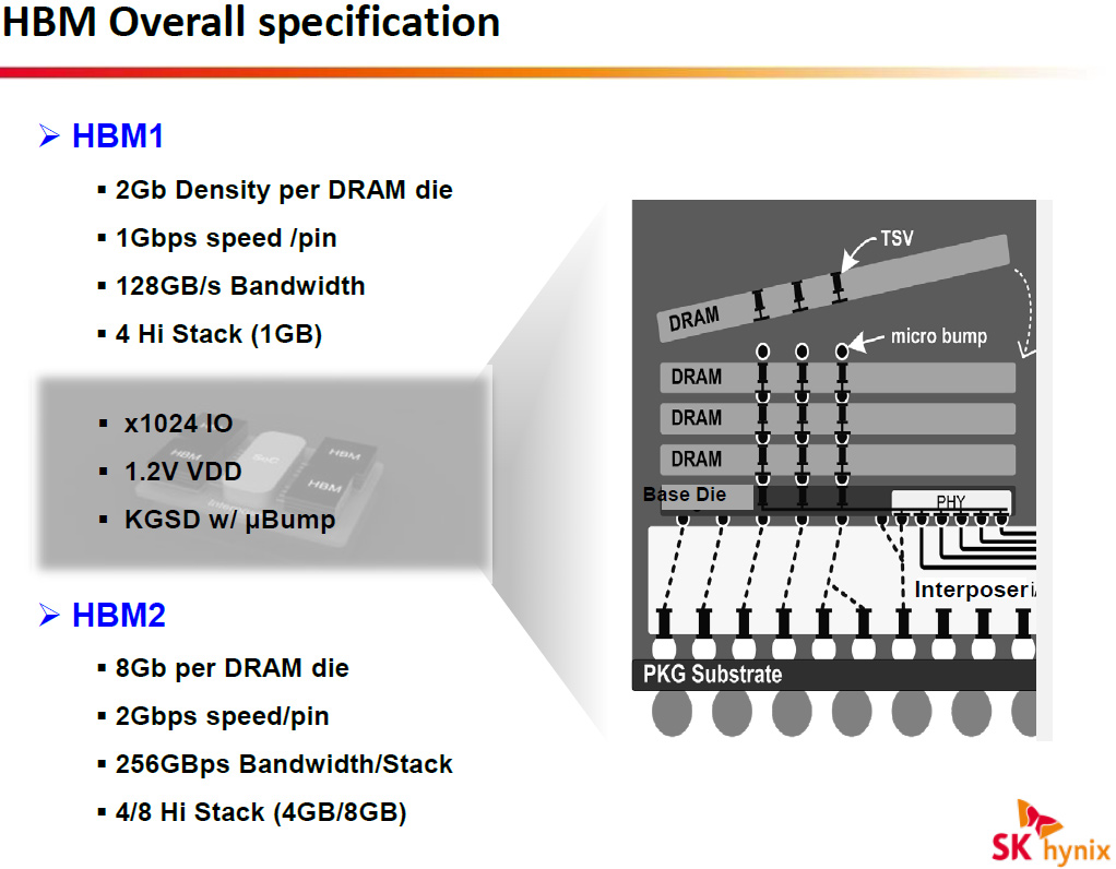
The first-generation HBM (HBM1) memory (which complies with JEDEC’s JESD235 standard) stacks four DRAM dies with two 128-bit channels per die on a base logic die, which results into a memory device with a 1024-bit interface. Each channel is similar to a standard DDR interface, but is completely independent and therefore each channel within one stack and even within one die can operate at different frequency, feature different timings and so on. HBM devices require 1.2V voltage.
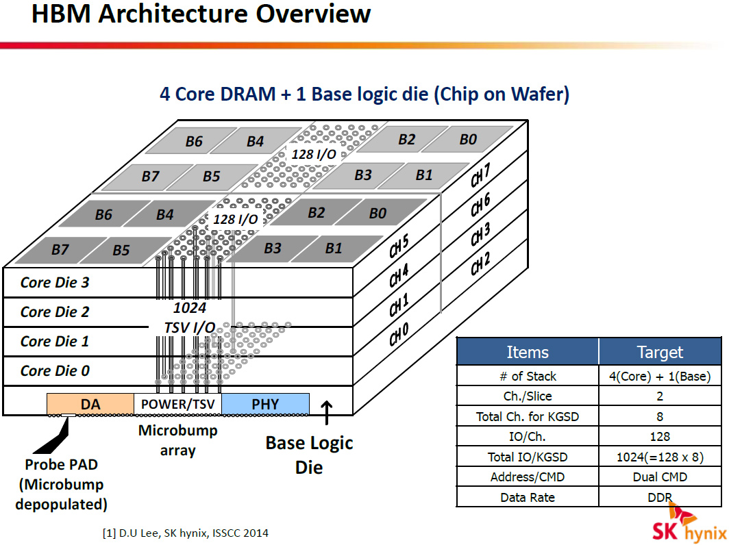
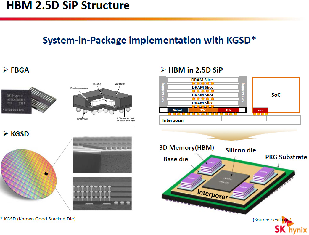
The first-gen HBM uses 2Gb DRAM dies and thus can form only 1GB 4Hi stack (4 high stack) packages. Each HBM 4Hi stack provides 128GB/s of bandwidth. HBM memory chips are tested before shipping to customers by SK Hynix. Each HBM 4Hi stack is placed on an interposer next to the graphics processing unit, for the first time in the industry. The first-gen HBM stacks are made using a proven 29nm fabrication process.
“AMD has pioneered the adoption of HBM1 technology in graphics applications achieving unprecedented memory bandwidth while reducing memory subsystem power” said Joe Macri, corporate vice president and product CTO at AMD, “Integrating AMD’s graphics processing unit and HBM1 on a single 2.5D silicon interposer represents a major step forward in high performance graphics applications”.
Even though the first-generation HBM has a number of limitations when it comes to the amount of stacks (only four layers are supported) and capacities of DRAM channels, AMD believes that unprecedented bandwidth provided by such chips – 512GB/s – will help it to significantly improve performance of its Radeon Fury X graphics solutions compared to current-gen solutions.
SK Hynix is shipping HBM to AMD today and plans to support demand for such memory from other customers.
Next year SK Hynix and other memory producers will start to manufacture second-generation HBM that will support up to eight memory stacks, higher DRAM capacities and clock-rates. HBM2 will allow to create 8GB memory chips with 256GB/s bandwidth per chip.

“High bandwidth memory technology is the first JEDEC standard memory targeted for interposer system-in-package applications, effectively breaking down the memory wall barrier through tight integration of DRAM and high performance processors” said Kevin Widmer, vice president of technical marketing at SK Hynix America. “The performance requirements of emerging graphics, computing and networking applications are driving the demand for High bandwidth memory.”
Discuss on our Facebook page, HERE.
KitGuru Says: Without any doubts, HBM is the biggest DRAM breakthrough in a decade. Unfortunately, the first-gen seems to have serious limitations, which may curtail performance of AMD’s Radeon R9 Fury-series. On the other hand, let’s wait and see how serious will those performance limitations be.

Your first choice kitguru Find Here