

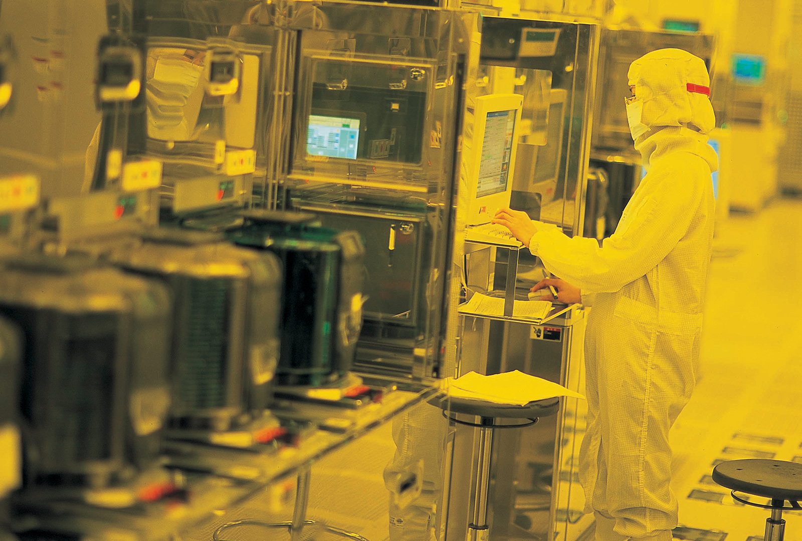
Taiwan Semiconductor Manufacturing Co. announced on Thursday that it had started volume production of chips using its 16nm FinFET manufacturing technology in the second quarter of 2015. The world’s largest contract maker of semiconductors is delivering the first batch of products made at 16nm node to its customers right now, according to chief executive of TSMC. The high-volume ramp of 16nm FinFET tech begins this quarter, on-track with expectations.
“We have begun volume production of 16 FinFET in second quarter,” said C.C. Wei, president and co-CEO of TSMC, during the company’s earnings conference call with investors and financial analysts. “Shipment has started this month. The high volume ramp in third quarter [will be] mostly contributed to revenue in fourth quarter this year.”
Previously TSMC said that high-volume production of chips using its 16nm FinFET (CLN16FF) process technology starts in the third quarter, with meaningful revenue contribution beginning in the Q4 2015. The current announcement confirms that high-volume ramp of TSMC’s first process technology with FinFETs [fin-shaped field-effect transistors] proceeds in accordance with the plans.

TSMC’s 16nm FinFET (CLN16FF), 16nm FinFET+ (CLN16FF+) and 16nm FinFET compact (CLN16FFC) fabrication processes all rely on metal back end of line (BEOL) interconnect flow of 20nm manufacturing technology. As a result, while the chips produced using TSMC’s 16nm tech cannot boast with leading-edge transistor density and have very high per-transistor costs, TSMC can ensure rather high yields with its new process.
“Since 16nm shares similar metal backend process with 20nm, our 16nm FinFET can benefit a lot from 20nm's learning,” said Mr. Wei. “We have already shipped more than half of a million CLN20SOC wafers by now, so our 16nm’s yield and defect density has been excellent. In fact, our 16nm FinFET has set a new record for progresses made in the defect density reduction.”
Because 16nm FinFET fabrication process is more universal than TSMC’s CLN20SOC, which was designed solely for mobile system-on-chips, more customers will use the new manufacturing technology. TSMC is aggressively expanding its 16nm capacities and is also converting some of its 20nm product lines to 16nm. The company expects wafer revenue for 16nm process to account over 20 per cent of its total wafer revenue next year.
“The ramping of our 16nm will be very steep, even steeper than our 20nm,” said Mr. Wei.

TSMC does not disclose names of its customers, but it is highly likely that the first company to get TSMC’s 16nm chips is Apple. It is possible that the lion’s share of TSMC’s 16nm capacities in Q3 2015 will be used to make Apple’s A9 chips for next-generation iPhone and iPad products. TSMC is expected to deliver the first high-volume batch of 16nm FinFET products in October. Initial next-gen smartphones from Apple will be based on semiconductors produced by Samsung Electronics using its 14nm LPE fabrication process.
Discuss on our Facebook page, HERE.
KitGuru Says: TSMC is over half of a year behind Samsung Foundry with volume production of chips using a FinFET process. Keeping in mind vast manufacturing capacities of TSMC, the company will probably beat Samsung in terms of volumes. However, when it comes to time-to-market, Samsung is clearly ahead of its rival.

This is confusing. GloFlo just gave up on 20nm wafers. Intel highly successful 14nm technology is a great standard, especially if Intel opens up their FABs to Intel’s partners. Now TSMC is going to 16nm while GloFlo is going to a 14nm and NVidia has made a deal with Samsung for 14nm for Pascal. I guess the difference is in locking their customers into a certain wafer size but who is going to bite? GloFlo lost a lot of time with working on 20nm.
apple are using samsung 14nm and TSMC 16nm for their new A8 or whatever. performance must be damn close. 2 nm we are talking smaller than a strand of DNA lol
->->->
>