

Taiwan Semiconductor Manufacturing Co. this week unveiled first details about its 10nm fabrication process at the TSMC Technology Symposium in the U.S. The official goals are slightly less ambitious than those discussed last year, but the general focus of TSMC’s 10nm manufacturing technology is clear: considerable increase of transistor density compared to 16nm FinFET tech.
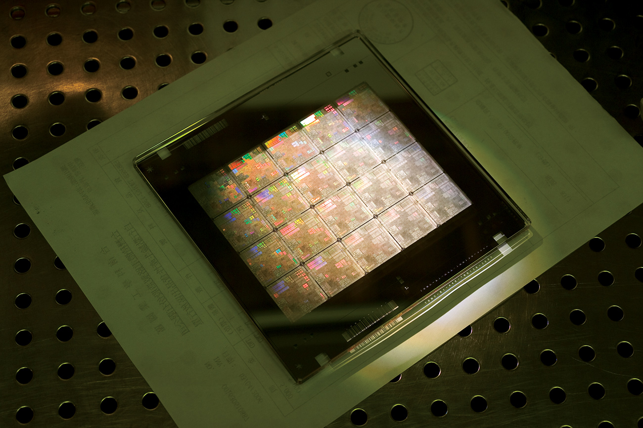
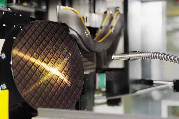
TSMC’s 10nm process technology will have 110 per cent higher logic density compared to the company’s 16nm FinFET+ (CLN16FF+) process tech, 20 per cent higher clock-rate potential at the same power and 40 per cent lower power consumption at the same frequency. Development of the manufacturing tech is proceeding as planned. TSMC demonstrated a 300mm wafer processed using its 10nm process containing 256MB SRAM memory ICs [integrated circuits] at the symposium, reports EETimes Europe.
Since TSMC’s 16nm FinFET manufacturing technologies rely on back-end-of-line interconnects (contacts, insulating layers, metal levels, and bonding sites) developed for the company’s 20nm process, geometries of chips produced using CLN16FF process are exactly the same as those of ICs made using CLN20SOC. Moreover, per-chip/per-gate costs of products made using TSMC’s 16nm FinFET are higher than those of chips produced using the company’s 20nm tech.
TSMC’s primary goal with 10nm process (CLN10FF) was to maximize logic densities so that to decrease per-chip and per-transistor costs of ICs made using the technology. 110 per cent higher logic density compared to the CLN16FF+ is a good achievement, even though it is lower compared to 125 per cent improvement discussed last summer.
Earlier this year TSMC indicated that its 10nm manufacturing tech will be a very long lasting node that will address multiple areas and thousands of devices. The company expects 10nm to contribute over 50 per cent of its wafer revenue in 2020.
TSMC plans to install equipment for risk production using 10nm process technology in one of its existing fabs this year. Trial production is expected to begin in Q4 2015. The company also plans to start construction of a brand-new fab to make 10nm chips in the second quarter of 2016. Volume production using 10nm process tech will commence in 2017.
Discuss on our Facebook page, HERE.
KitGuru Says: TSMC is behind its rivals when it comes to production using a FinFET technology, hence, the firm is attempting to speed up 10nm development and mass production. The fact that the firm has adjusted its goals indicates that its CLN10FF is still a work in progress, which is okay since TSMC has two years to perfect the tech.

tyut . true that Patricia `s report is impossible… on wednesday I bought Saab 99 Turbo since I been making $8569 thiss month and also ten/k this past month
. it’s actualy my favourite-work I’ve had . I began this three months/ago and pretty much straight away was earning more than $75… p/h . you could try here HERE’S MORE DETAIL
There are a LOT of you smeggers who bought a Saab 99 Turbo on Wednesday, despite the fact Saab no longer produce any cars… if you bought second hand you have been had mate! Also you all seem to have made $8569 ‘thiss’ month, that’s really lovely for you all and thank you for rubbing it in our faces you lowlife scum 🙂