
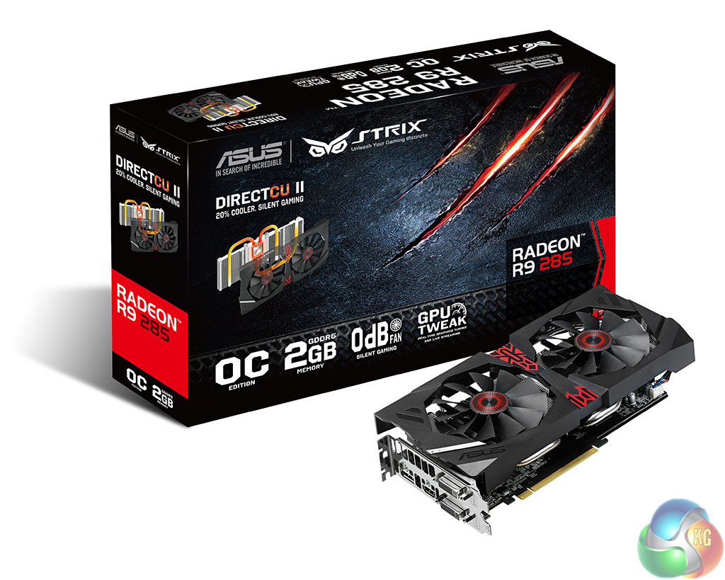
We didn't receive a retail sample for our review today, but we managed to get the image above directly from ASUS. No idea of the accessories inside, but you should expect a couple of power/signal converter cables and some literature on the product.
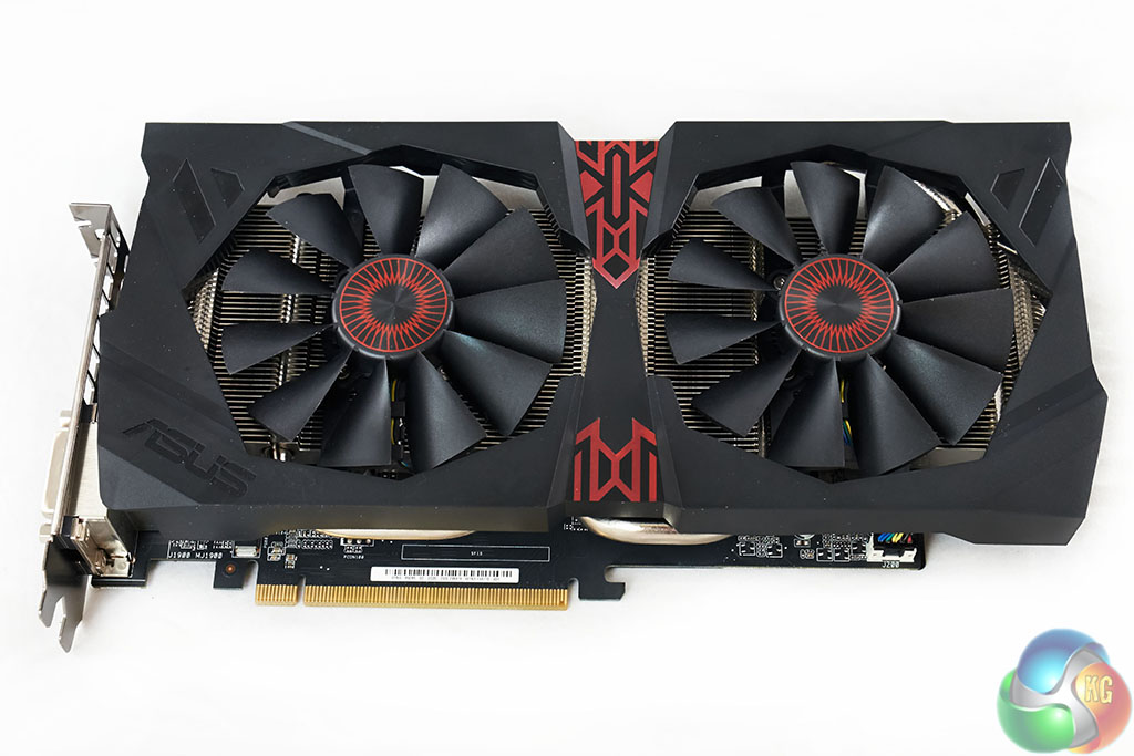
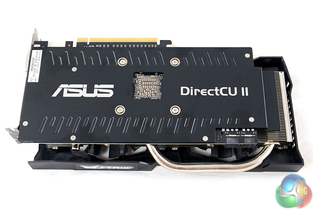
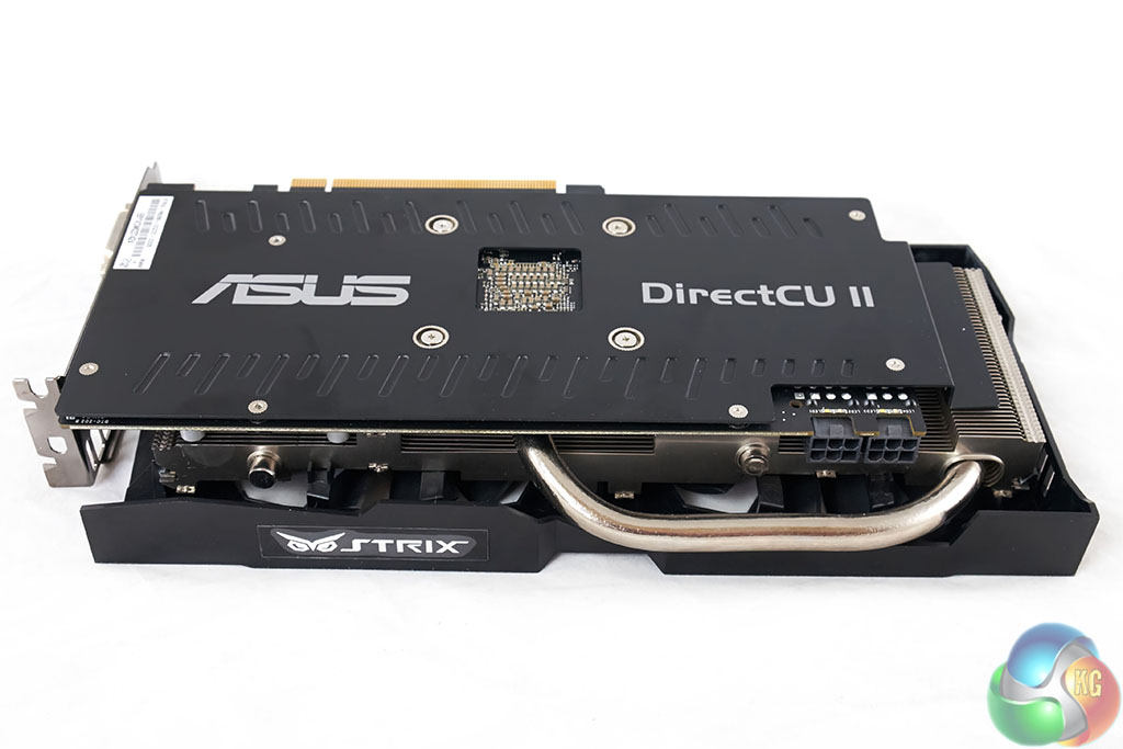
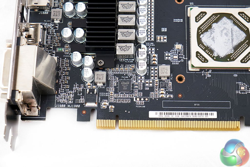
The R9 285 STRIX card is nicely finished and doesn't feature any text branding on the front. The ‘OWL' style artwork is visible. The rear of the card features a backplate, with ASUS and Direct CU II naming. The STRIX utilises an 8 phase power system.
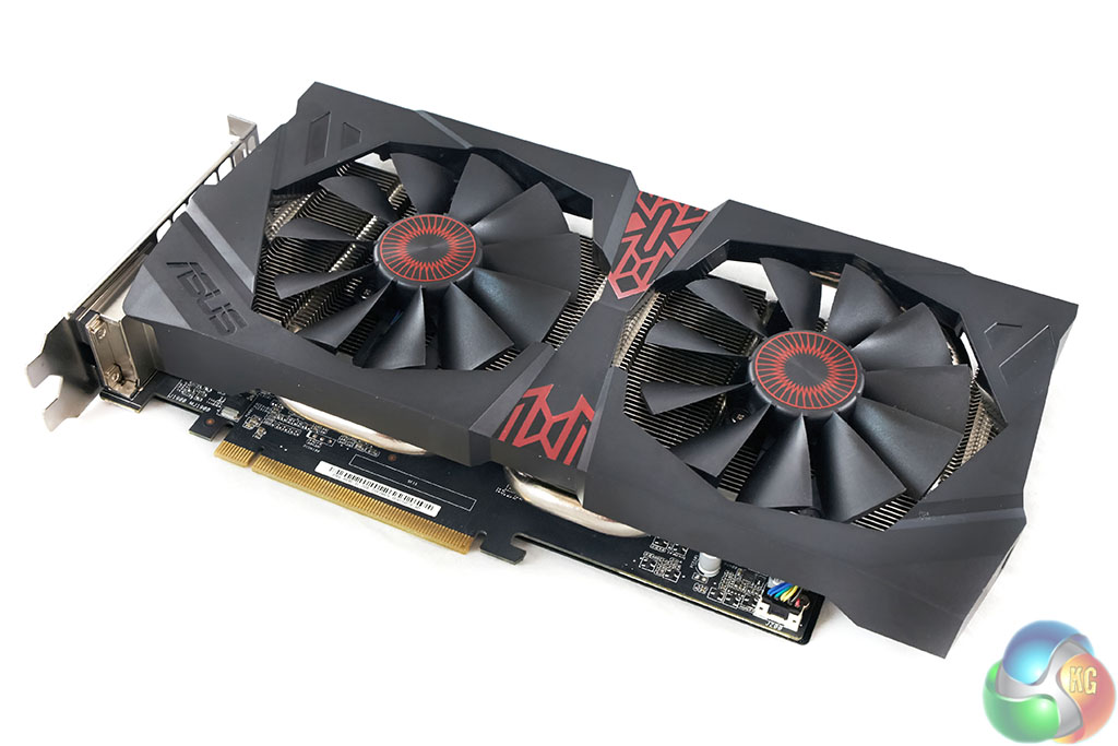
The ASUS STRIX looks good from all angles, and there is a hefty heatpipe visible along the top of the cooler. The fans are said to deactivate under specific load demands – but we will look at this later in the review. No Crossfire headers on this card – it will work directly in the slot with more than one card, without a connector. Bridgeless Crossfire has been a welcome feature on the 290 series now for some time.
It takes power from two 6 pin power connectors as seen in the images above.
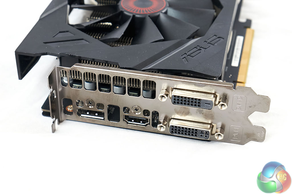
The ASUS Strix card has two DVI connectors (DVI-D and DVI-I), a full sized DisplayPort connector and a HDMI connector.
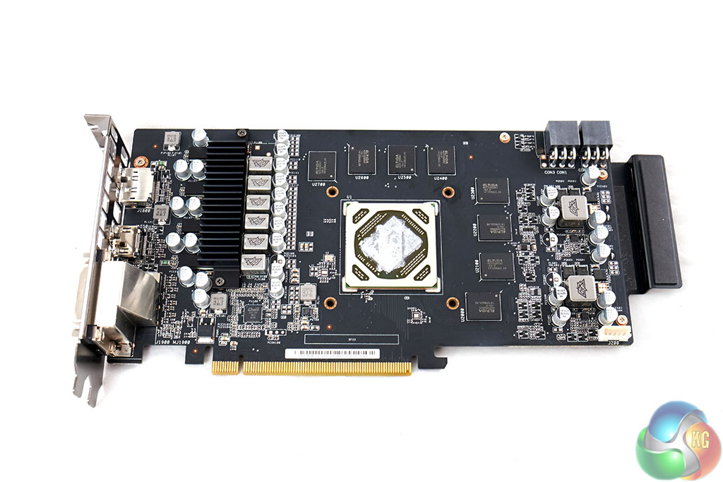
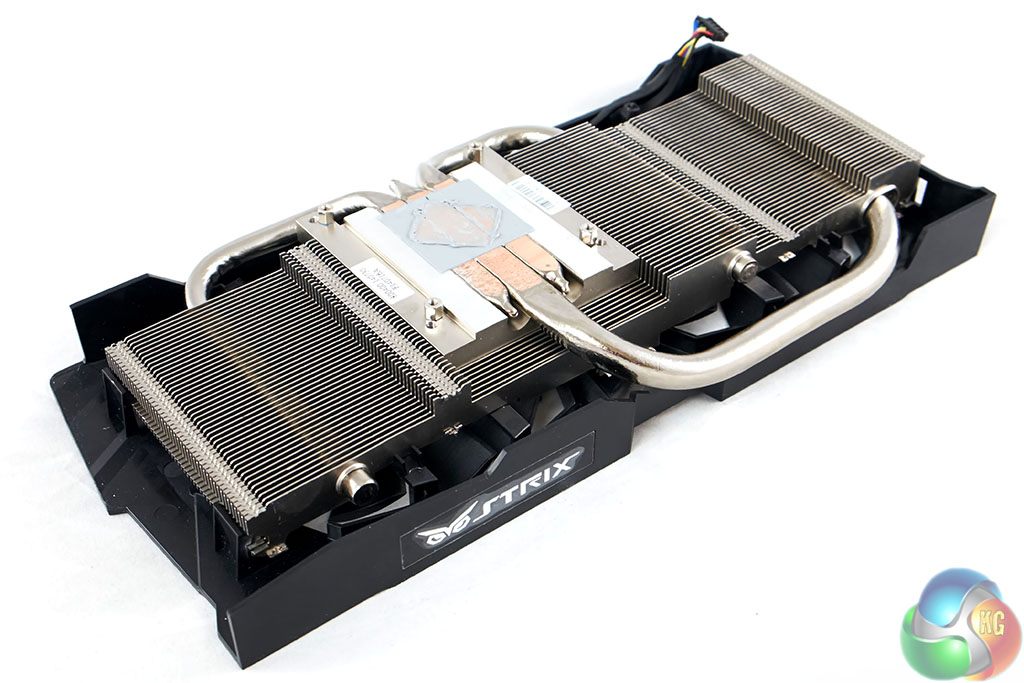
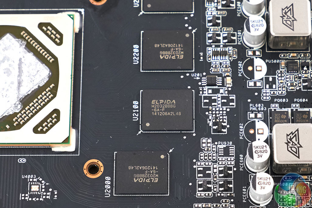
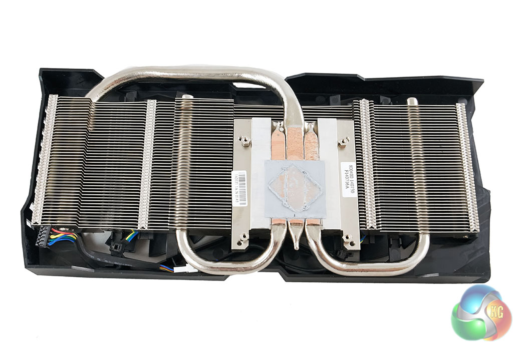
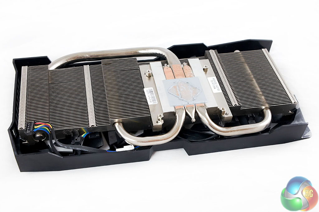
The Asus R9 285 Strix is using Elpida GDDR5 memory. The cooler is a substantial design incorporating three thick heatpipes which run into two separate racks of aluminum fins on either side of the copper core. The cooler is using direct touch methodology. Asus are using Super Alloy Chokes on the PCB to eliminate any potential ‘buzzing'.
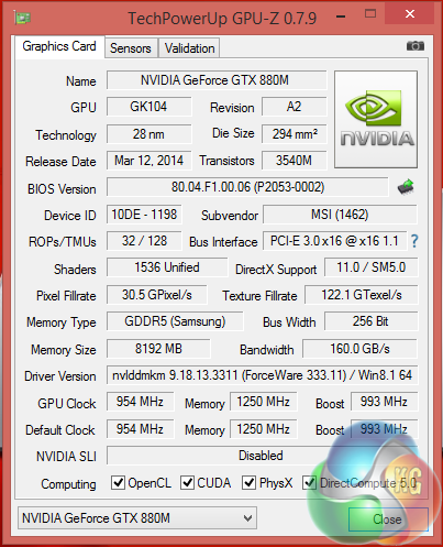
Special thanks go to Mike over at Techpowerup for getting me a new beta version of GPUz with full support for the Tonga hardware in time for this review. We can see that ASUS have clocked the card at 954mhz. Memory is running at 1,375 mhz (5.5Gbps effective). The card is equipped with 32 ROPs, 112 Texture units and 1,792 Stream Processors – the same configuration as the R9 280.
As mentioned on the previous page AMD have dropped the memory count down from 3GB to 2GB in the update from R9 280 to R9 285. There will be 4GB versions of the R9 285 at a later date however.
The memory interface is also reduced from 384 bit to 256 bit.
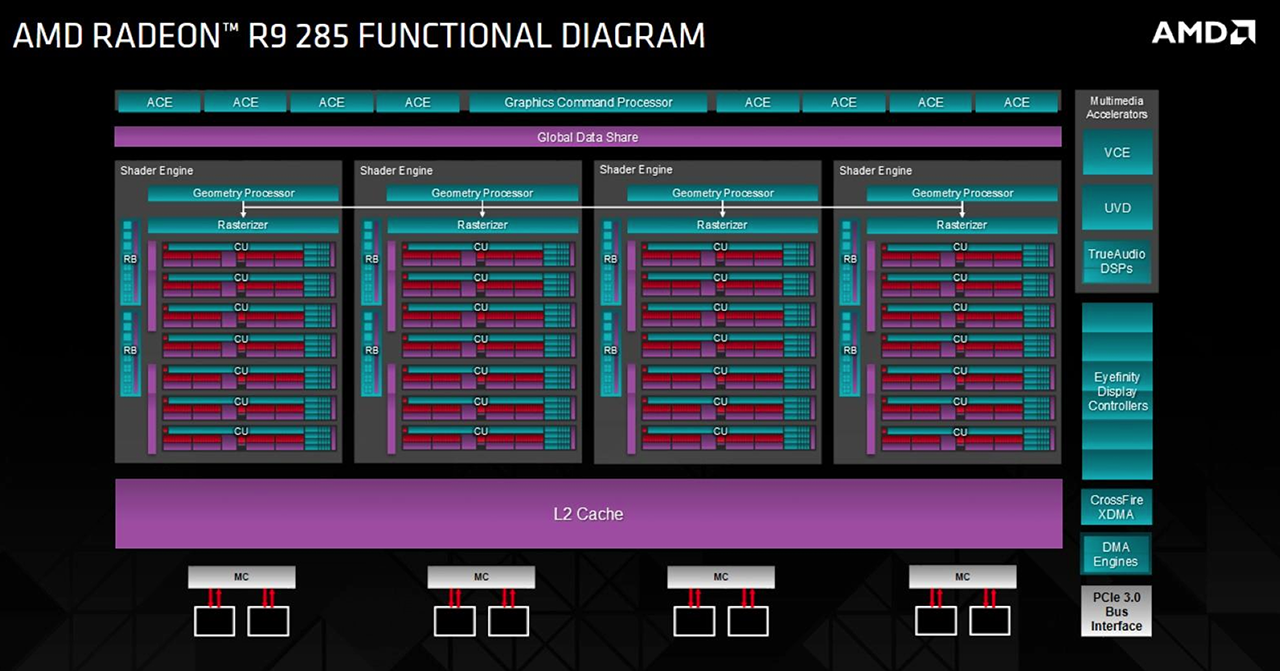
A functional diagram of the R9 285 hardware. Without getting bogged down in discussions of architecture I spoke with Evan Groenke, Senior Product Manager for AMD in Ontario a couple of days before this launch article.
He explained that there was a significant level of technology that went into making a highly efficient 256 bit product (compared to the 384 bit R9 280 before it).
AMD are using a lossless delta colour compression (DCC) algorithm to get a 40% efficiency improvement over the 384 bit product. The colour data is being stored in a lossless compressed format using delta encoding. Evan explained that this has no effect on image quality and is done automatically on the fly.
He also explained that geometry performance has improved dramatically. Their 4xPrim rate has improved tessellation (2-4x) when compared to the R9 280. They have managed to enhance performance from improving their work distribution between geometry front end units and improved vertex re-use when dealing with many small triangles.
Multimedia areas have been improved including a new Unified Video Decoder which provides a full fixed function decode engine with support for H.264, VC-1, MPEG4, MPEG2 and MJPEG. It also adds support for high frame rate 4K H.264 content (High Profile Level 5.2). The new Video Coding Engine provides (up to) 12x faster than real time encoding for full HD and support for 4K resolutions.