

The Chief Engineer at Kioxia, Shigeo Oshima, recently gave a presentation at VLSI Symposium 2020 where he talked about the company's plans for a “Wafer-Level SSD”, a potentially game changing approach to storage production.
The process of creating an SSD device is usually a long and complicated one. It starts with a wafer being manufactured in a factory and later being cut into individual chips that are packaged into SSDs and finally installed in a computer. However, Kioxia wants to see a change to the long and usually expensive process of manufacturing SSDs – through the introduction of “Wafer-Level SSD”.
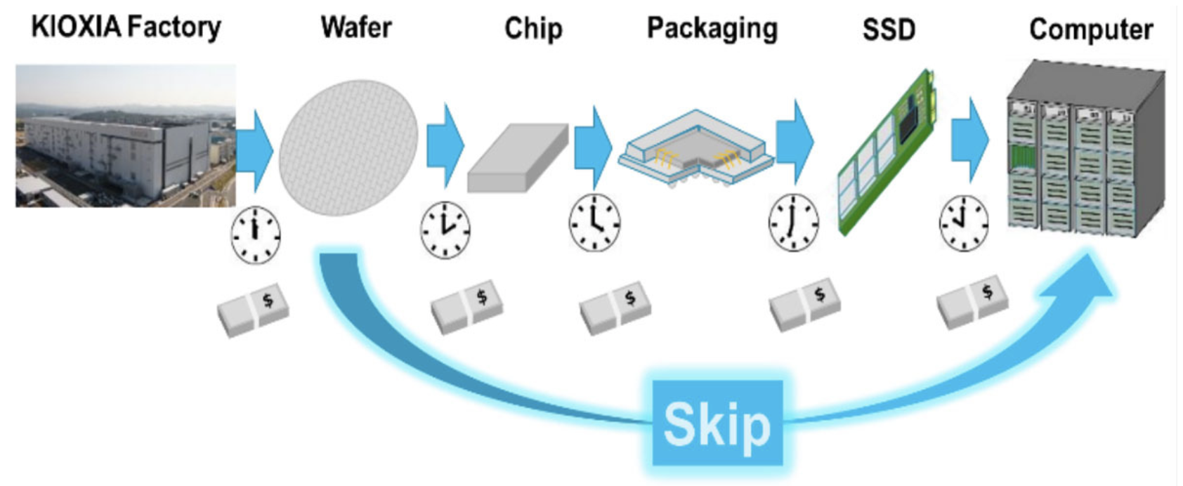
Wafer-Level SSD technology still has a long way to go before it can manifest itself in devices ready for the market. But, if Kioxia is able to develop the technology and make it a reality, it would mean big cost savings when manufacturing SSDs, since many steps of production could be cut out. The technology also has the potential to be used for “wafer stacking”, with the prospective benefits of immensely enhanced performance in SSDs.
The details we have at present are based on a Japanese report from ‘My Navi‘ but hopefully we'll hear more about the development of this later in the year.
Kitguru says: The concept of Wafer-Level SSDs is still in its infancy, but could mean better performance and lower costs for SSDs in the future. What are your thoughts on Wafer-Level SSDs?