

The first specifications as well as a block-diagram of AMD’s next-generation code-named “Carrizo” accelerated processing unit (APU) have been published by a web-site. Despite expectations, the “Carrizo” will not support high-bandwidth memory (HBM) technologies, at least, in its mainstream implementation. Nonetheless, the new chip will carry a fair amount of innovations compared to the current-gen Kaveri APU. Unfortunately, there are some cut-downs too.
The structure
Based on an excerpt from an alleged AMD’s document published by Chinese VR-Zone web-site, AMD’s “Carrizo” chip will be structurally similar to its predecessors, which means that all performance improvements will be a result of architectural enhancements, not from increases of execution units. As expected, starting from the “Carrizo” accelerated processing unit AMD will offer system-on-chips (SoC) that will place both APU and core-logic set (FCH, Fusion controller hub) onto the same piece of substrate, which will help to shrink mobile and all-in-one PC form-factors.
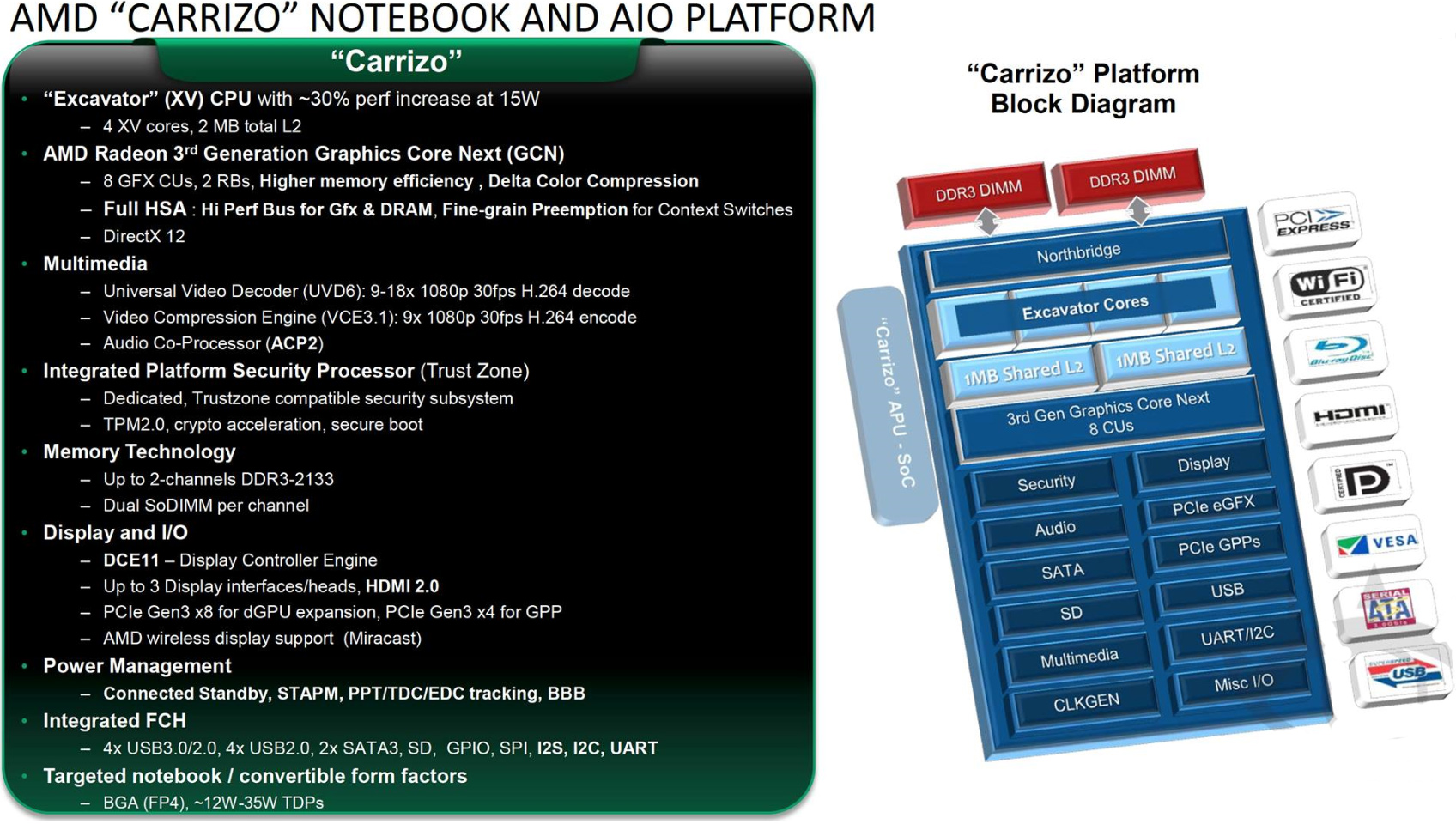
AMD Fusion “Carrizo” accelerated processing unit will feature two dual-core AMD “Excavator” (XV) modules with 2MB L2 cache (1MB of cache per module, 512KB of L2 cache per core), AMD Radeon graphics based on the third-generation graphics core next architecture (GCN 3.0) architecture with eight compute units (512 stream processors in total), an integrated dual-channel DDR3 memory controller, a new special high-performance bus to connect x86 cores to graphics cores and DRAM, further HSA [heterogeneous system architecture] enhancements, PCI Express 3.0 controller as well as all-new multimedia and input/output engines.
AMD’s “Carrizo” SoCs will come with integrated I/O controller that will support PCI Express, USB 3.0, Serial ATA-6Gb/s, SD, GPIO, I2S, I2C, UART, an integrated clock-generator and so on. Such system-on-chips will have thermal-design power between 12W and 35W.
The Excavator and cut-down L2 cache
According to the published slide, AMD expects its “Excavator” cores to provide 30 per cent performance increase presumably compared to the current-gen “Steamroller” cores at 15W thermal design power. Typically such predictions have little to do with reality since they are based on virtual simulations, not real tests. However, keeping in mind significant architectural enhancements of the “Excavator” compared to the “Steamroller”, it is possible that the upcoming x86 cores from AMD will perform noticeably better compared to the current ones.
For some reason AMD decided to cut-down L2 cache of the new APUs to 2MB from 4MB on the contemporary accelerated processing units (even 15W quad-core A10 “Kaveri” chips feature 4MB of L2). Cutting-down L2 cache without adding large L3 cache will almost inevitably result in performance degradation in single-threaded applications.
The exact reason why AMD decided to decrease L2 cache sizes is unknown. Perhaps, this was done because the “Excavator” cores are considerably larger than the “Steamroller” cores and AMD needed to keep the die size of Carrizo small enough to ensure the same manufacturing costs, which is why it decided to reduce the level-two cache size. Maybe, AMD’s new high-speed interconnections and improved memory controller somehow reduce the importance of large caches.
Hopefully, AMD knows what it is doing and the “Carrizo” APU will not be slower than the “Kaveri” chip in certain applications that require big caches.
AMD Radeon and GCN 3
The forthcoming APU will also feature a new AMD Radeon graphics engine based on the third-generation GCN architecture. The new architecture will feature a number of enhancements, including fine-grain pre-emption for context switches (should increase efficiency of heterogeneous computing by making context switches more flexible) as well as delta-color compression (an image compression technique that encodes a row of pixels by replacing their colour information with values that represent difference between subsequent pixels [e.g. if one pixel in RGB format is 255:0:0, the other one is 255:1:1, the third one is 255:2:0, then with delta compression the sequence can be represented as 255:0:0, 0:1:1, 0:1:-1].
The GCN 3 is also projected to support DirectX 12 application programming interface, but it is unclear whether it will actually support all the new capabilities of the API, or will be just compatible with the API while supporting DirectX 11.2 feature level.
Multimedia, I/O and power management
The “Carrizo” APU will also feature enhanced multimedia, security and I/O capabilities.
The new chip will come with universal video decoder 6.0 (UVD6), video encoder engine 3.1 (VCE3.1) and audio co-processor 2 (ACP2). At present there is no word about support for ultra-high-definition (UVD) video codecs, such as H.265/HEVC or VP9. Looks like decoding of 4K video will not be a strong side of the new APU from AMD.
Despite of the fact that there will be no hardware support of UHD decoding, the Carrizo will support HDMI 2.0 output (which means it will be able to display 3840*2160 video with 120Hz refresh rate, stereo-3D UHD video and so on). The APU will support up to three displays.
In addition to TrustZone technology, AMD’s new chip will also support TPM 2.0, crypto acceleration and secure boot, the first time for AMD.
As expected, the “Carrizo” will also support advanced power management capabilities, including connected standby, STAPM, PPT/TDC/EDC tracking and so on.
Some thoughts
Since AMD’s “Carrizo” accelerated processing unit will be made using the same 28nm process technology as the “Kaveri”, it was illogical to expect AMD to significantly enhance its performance by increasing the number of x86 cores or stream processors because of the manufacturing costs reason. Unfortunately, improvements on the micro-architecture levels no longer bring breakthrough performance boosts. As a result, the “Carrizo” will not change the situation on the market of microprocessors any significantly. It will be somewhat faster than the predecessor (in applications that don't take advantage of large caches), but Intel’s “Broadwell” and “Skylake” processors will also be somewhat faster than the existing “Haswell” offerings.
Discuss on our Facebook page, HERE.
KitGuru Says: For several years now AMD is trying to change the rules of the game on the market of microprocessors. Instead of rapidly advancing its x86 micro-architecture, the company is trying to persuade the industry to use GPU compute technologies everywhere. Since x86 performance remains a very important aspect, AMD’s chips are gradually losing popularity among those, who need truly high performance in all applications.
[1] Level of secondary cache was anticipated for sever loads, not desktop, a reducation in such will increase performance, [2] “GCN 3.0″ is a figment of vr’s imagination, no such designation exists at AMD [3] quad-hd hardware support is categorically supported [4] ” 12-35w tdp means this is a bottom-ish bin, and may have god knows what fused off [5] I don’t think i can bring myself to give much of a shit; 15h is dead, AMD killed it at least a year ago now – for the the love of mike will AMD bring out K12 and Kx cores already?
“CPU ~30% performance increase”
which stems from what, clock speed increase? IPC increase? An extra CPU core?!?