

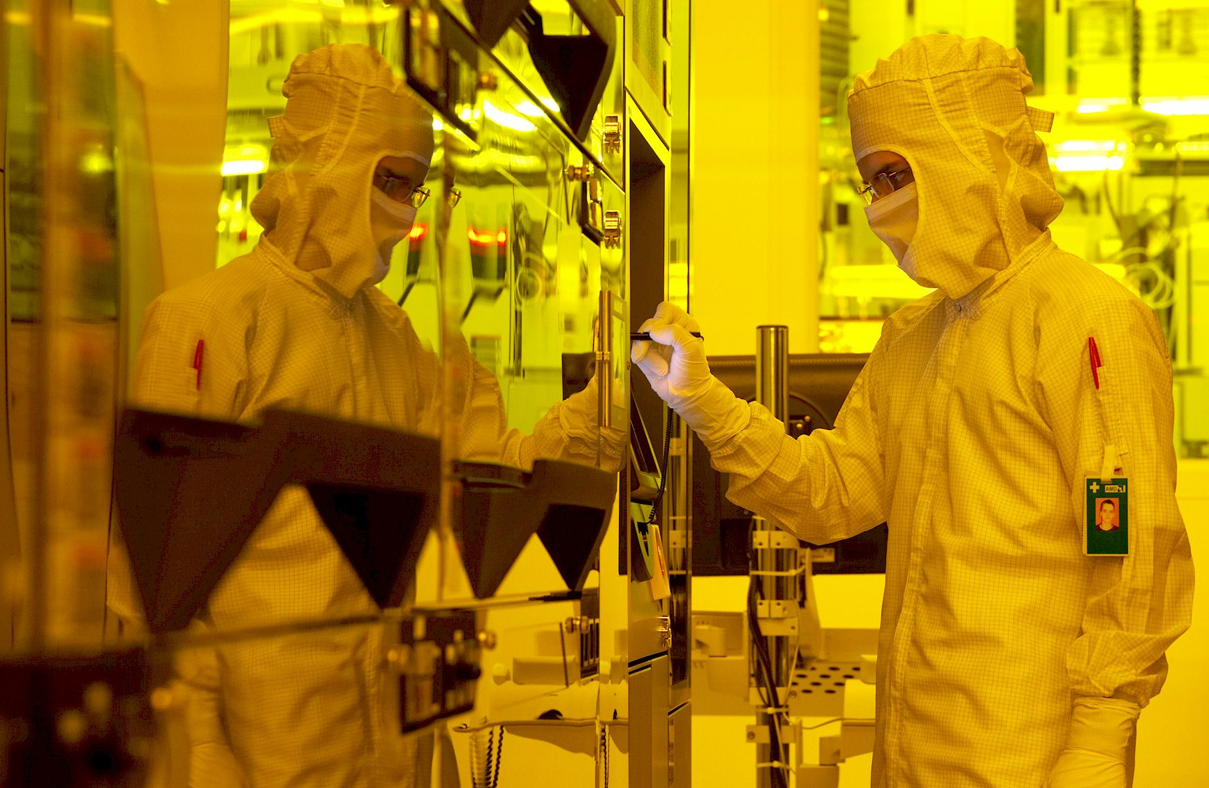
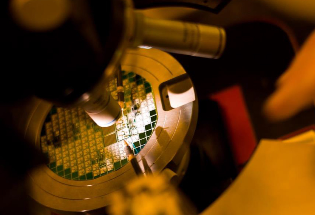
GlobalFoundries on Monday introduced a family of fully-depleted silicon-on-insulator (FD-SOI) manufacturing technologies designed for customers seeking high performance and low design costs. The new fabrication processes promise to deliver performance of next-generation technologies with FinFET transistors, but at costs comparable to those of existing processes.
GlobalFoundries calls its new family of process technologies 22FDX and will offer four versions of the process designed for different kinds of applications. Despite of the fact that GlobalFoundries classifies its technology as a “22nm”, the process has nothing to do with 22nm production process used by Intel Corp. or other chipmakers.
The 22FDX uses back-end-of-line (BEOL) interconnect flow of STMicroelectronics’ 28nm FD-SOI as well as front-end of line (FEOL) of STM’s 14nm FD-SOI. GlobalFoundries’ 22FDX is a planar technology that sports 50 per cent fewer immersion lithography layers than foundry FinFET technologies. It also does not require double-patterning anywhere, which simplifies chip design. According to GlobalFoundries, the 22FDX platform delivers a 20 per cent smaller die size and 10 per cent fewer masks than 28nm.
Since 22nm FD-SOI is planar process and does not require double-patterning, it will be cheap enough even for small companies. One mainstrem FinFET IC [integrated circuit] costs $80 to $90 to design, which is a lot of money. By contrast, it will cost around $30 million to design a planar chip. It will also be less expensive to manufacture actual products using 22nm FD-SOI than using 16nm or 14nm FinFET processes.
An important feature of GlobalFoundries 22FDX is software-control of transistor characteristics to achieve real time tradeoff between static power, dynamic power and performance.
“The 22FDX platform enables our customers to deliver differentiated products with the best balance of power, performance and cost,” said Sanjay Jha, chief executive officer of GlobalFoundries. “In an industry first, 22FDX provides real-time system software control of transistor characteristics: the system designer can dynamically balance power, performance, and leakage. Additionally, for RF and analog integration, the platform delivers best scaling combined with highest energy efficiency.”
The GlobalFoundries 22FDX family of process technologies consists of four options:
- 22FD-ulp: Designed for inexpensive system-on-chips used for mobile applications. The process uses body-biasing, and delivers greater than 70 per cent power reduction compared to 0.9V 28nm HKMG. Moreover, select chips made using 22FD-ulp will be able to operate at 0.4V.
- 22FD-uhp: Designed for networking applications with analog integration. The manufacturing tech offers forward body-bias, application optimized metal stacks, and support for 0.95V overdrive.
- 22FD-ull: The process tech is aimed at Internet-of-Things devices and features leakage of as low as 1pa/um. The manufacturing tech sports flexible body-biasing and other capabilities designed to reduce power consumption.
- 22FD-rfa: The process tech developed specifically for radio frequency and analog applications. The technology will be used to make high-volume RF applications such as LTE-A cellular transceivers, high order MIMO WiFi combo chips, and millimeter wave radar.
GlobalFoundries’ 22FDX process technologies are expected to be used by multiple designers of chips and are supported by various IP providers. Among supporters of the manufacturing processes are ARM, Imagination Technologies, Freescale, IBS, STMicroelectronics, VeriSilicon and other. Design starter kits and early versions of process design kits (PDKs) are available now with risk production starting in the second half of 2016. Mass production of 22FDX chips will start in the second half of 2017.
Discuss on our Facebook page, HERE.
KitGuru Says: As expected, GlobalFoundries’ 22nm FD-SOI process technology will not be suitable for microprocessors, graphics processing units or high-end mobile application processors. While smaller vendors will probably take advantage of increased performance, low power consumption and low cost of design, leading chip designers will hardly ever use 22nm FD-SOI for their mass products.

Really GloFo? IBM hands you FD-SOI with FinFET combined in for ultimate performance and power consumption, literally the best of both worlds (See Power 8 chips), and you just regress it to planar FDSOI? Do the stupid moves not end with this foundry?
I check up on draft that aforesaid 19958$@mt4
bj…..
http://www.WorldCareersDevelopersBlue/blog/cold...