

One of the advantages that some of Intel Corp.’s integrated graphics processors (IGPs) have compared to AMD’s IGPs is a large level four cache that is used to store frequently used data. While at present AMD’s integrate graphics adapters are still faster compared to Intel’s, in the future the latter may become considerably more competitive. In a bid to ensure that its IGPs are the fastest on the market, AMD reportedly plans to equip them with high-bandwidth memory that will act like cache.
Bitsandchips.it reports that AMD intends to use stacked on-package high-bandwidth memory (HBM) on its next-generation code-named Carrizo accelerated processing units (APUs). No details have been revealed, but usage of HBM will significantly improve performance in graphics and other memory bandwidth-dependent applications, which will make AMD’s APUs much more competitive than they are today.
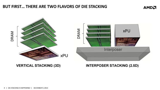
The HBM DRAM is tightly coupled to the host compute die with a distributed interface. The interface is divided into independent channels. Each channel interface maintains a 128-bit data bus operating at DDR data rates. Earlier this year it transpired that AMD has worked with SK Hynix to ensure compatibility of its future chips with industry-standard HBM. A 2133MHz HBM device with 128-bit interface can offer up to 34.1GB/s of bandwidth, two of such devices could provide up to 68.2GB/s of bandwidth, which is two times higher compared to today’s memory sub-systems of AMD APUs. An HBM device could be integrated into a chip by stacking it vertically or just placed next to a chip onto the same piece of substrate. AMD will likely use the second approach.
Micron Technology, as well as a number of its partners, have designed their own proprietary version of HBM called the hybrid memory cube (HMC). The first commercial HMC 1.0 implementation is available from Micron in a 2GB density with an unprecedented 160GB/s of memory bandwidth, while running at 10Gb/s per lane data-rate. The new HMC 2.0 specification supports increased data rate speeds advancing short-reach (SR) performance up to 30Gb/s, allowing to boost peak bandwidth of a single memory cube up to 480GB/s.
It is not a secret that AMD, Intel and Nvidia are exploring HBM DRAM and plan to use it for their next-generation graphics processing units as well as Xeon Phi co-processors. Theoretically, AMD could use the HBM technology with its APUs as well since it is more cost-efficient than integrating large caches into chips or using embedded DRAM.
AMD did not comment on the news-story.
Discuss on our Facebook page, HERE.
KitGuru Says: While it is logical for AMD to use HBM, it should be noted that this will increase the costs of its APUs and will require AMD to take additional risks. At the same time, HBM will unlikely dramatically boost performance of AMD’s IGPs unless the company plans to significantly increase the amount of stream processors and other execution units in the Carrizo. Keeping in mind that the Carrizo will be made using 28nm process technology, it is highly unlikely that the chip will be significantly different (i.e., more powerful) compared to today’s Kaveri APU.

Could be both performance/cost related and power related, hard to tell without details and costs. Kaveri APU gaming performance scales well with RAM speed even up to DDR3-2400, so on-die fast RAM could offer the gaming performance of fast RAM with normal RAM. On mobile, where fast RAM is harder to get and costs matter more, that would certainly be important. On-die RAM can also be more power optimised and so save compared to fast RAM.
I’m just speculating, but it could be a good way forward. Certainly AMD APU’s have felt memory bottlenecked up till now.