

Some technical diagrams for the upcoming AMD X399 and a would-be X390 chipset have made a splash on the internet, it seems.
A post on an AMD subreddit included some very convincing chipset block diagrams showing off what looks like the X399 and X390 chipsets, and even a board layout for the latter. AMD, having presented Naples to the public a couple of weeks ago seemed scant on details. Now, if we consider the post a legitimate “reveal”, AMD seems to be packing some serious heat under the hood for the would-be Datacenter- and Workstation-class CPUs.
According to the diagrams we have a clearer picture of the X399 chipset for the upcoming Naples CPU, while X390 is a single-socket implementation of a similar design – the much talked-about single-socket implementation of said Naples. The leak may have also spilled the beans on the naming scheme for the CPUs, with Naples' SP3 dual sockets labeled RZ4700 (presumably a Ryzen 4700 CPU), and an RZ2700 CPU (again, presumably Ryzen 2700) for the single SP3r2-socket SKU.
The RZ4700 “Naples” and X399 chipset:
The dual socket SP3 configuration provides according to AMD, a whopping 128 PCIe 3.0 lanes, half of which are taken up by the Infinity Fabric interconnect between the two CPUs, 16 lanes dedicated to dual 10GbE (fiber?) connectors, SSD storage (8+4 lanes) and and the rest dedicated for compute-intensive GPU tasks on switched PCIe/GPU slots. On top of that, the diagram describes eight dual-channel memory controllers on each MCM, each driving ECC DIMMs of up to 32GB each (speed rating not specified, but we've heard rumours of a “tame” DDR4 2400) for a theoretical maximum of 1TB DDR4 ECC, on the dual-CPU configuration.
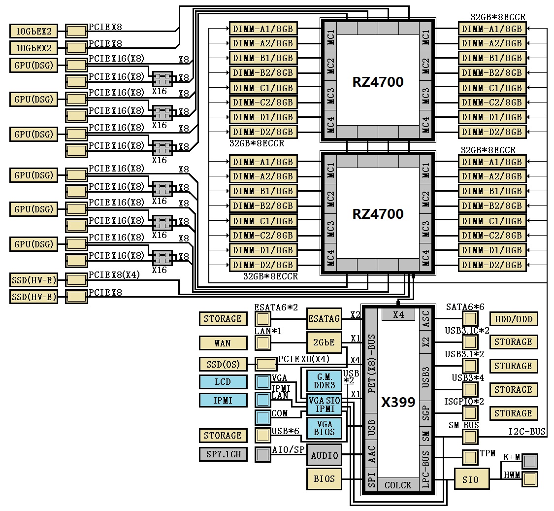
Apart from the list of features on the Naples CPU, X399 connects to the CPU cluster through four PCIe lanes and provides additional bandwidth and connectivity equivalent to old-school southbridges: legacy IO, integrated 7.1 audio, BIOS, SATA III (x6), USB 3.1C(x6), USB 3.1(x6), USB 3.0(x6), eSATA(x2), USB 2.0(x6), GPIO, SM-BUS, I2C, 2Gb ethernet, integrated VGA (and DDR3 graphics memory). It also reserves 8 PCIe lanes for a bootable PCIe SSD and sports a TPM module for secure computing.
The RZ2700 and X390 chipset:
The single-socket SP3r2 implementation for RZ2700 differs from its presumed big brother, providing higher integration of features and fusing a lot of the southbridge functionality into the CPU package. For example, the RZ2700 will sport a quad memory controller, addressing what seems to be a maximum 256GB of ECC DDR4-2666, but also include the USB 3.1 controller (3.1C x1, 3.1A x2), some standard I/O, TPU, EPU, I2C bus controller and integrated 7.1 channel audio. It drives a total of 48 PCIe lanes, four of which are reserved for the chipset interconnect, and the remainder 44 lanes distributed among a myriad of features like dual 10GbE, M.2 connector (for an OS SSD), and PCIe slots galore for solid state graphics or more storage.

The X390 chipset transfers a lot of circuitry to the CPU package, while providing 16-lane PCIe 2.0 connectivity for a range of storage/high-bandwidth options (eSATA 6Gb, PATA, a PCIe 16x/4x slot, dual GbE, FireWire A x2, FireWire B x1), SGPIO, SATA III (x6) and U.2 (4 lanes).
The motherboard diagram describes an EATX form factor sporting 3 PCIe 3.0 16x slots, one PCIe 2.0 16x/4x slot, M.2 (up to 110mm in length for Enterprise-class SSDs), dual Intel I211AT GbE controllers, six SATA III 6Gb/s connections, 8 DIMM slots for DDR4 2666.
KitGuru Says: At the end of the day, these leaks seem legit and give credit to AMD's assault on Intel, now in the Datacenter and Uniprocessor Server/Workstation space.

Its going to be nice to have a fat amd chip and board keepin’ my room toasty at night rendering everything. I will buy the shit out of X390 and that thicc ass 16 core cpu, yummy!!!
Naming is curious.
Boeing named their first conceptual supersonic transport contender from the 60’s as “2707” as an implied 2nd level above their first commercial subsonic jet “707”, I guess 1707 wouldn’t have sounded right. Of they cancelled the SST program due to Congress cutting funds over potential environmental impacts.
Anyway, a “Ryzen 2700” makes me think of Ryzen 7 1700, just double cores: at 3GHz base with 3.7GHz boost, 16c-32t can manage around 130W– but that won’t be the rated TDP since it wouldn’t account for future releases at either higher frequencies or more cores. Therefore the claimed 150-200W TDP bracket makes sense. Especially if doubling up the 95W model gets 190W.
Google is paying 97$ per hour! Work for few hours and have longer with friends & family! !mj217d:
On tuesday I got a great new Land Rover Range Rover from having earned $8752 this last four weeks.. Its the most-financialy rewarding I’ve had.. It sounds unbelievable but you wont forgive yourself if you don’t check it
!mj217d:
➽➽
➽➽;➽➽ http://GoogleFinancialJobsCash217HomeBankGetPay$97Hour… ★★✫★★✫★★✫★★✫★★✫★★✫★★✫★★✫★★✫★★✫★★✫★★✫★★✫★★✫★★✫★★✫★★✫★★:::::!mj217d:….,……..
AMD already showed their naming scheme, having these cpus belonging to that same naming scheme would mess it up as ot would sound like the chips are 2nd and 4th gen chips.
As for the Chipset naming, seems like AMDs decided its gonna screw over Intel by using the 370/390/350 namings.
I will wait for real life pricings and stuff before jumping to any conclusions
I’d say it’d be the same 8 cores, but improved IPC and clock speeds, making it suitable to use quad-channel DDR4 with.
Google is paying 97$ per hour! Work for few hours and have longer with friends & family! !mj138d:
On tuesday I got a great new Land Rover Range Rover from having earned $8752 this last four weeks.. Its the most-financialy rewarding I’ve had.. It sounds unbelievable but you wont forgive yourself if you don’t check it
!mj138d:
➽➽
➽➽;➽➽ http://GoogleFinancialJobsCash138MediaTeamGetPay$97Hour… ★★✫★★✫★★✫★★✫★★✫★★✫★★✫★★✫★★✫★★✫★★✫★★✫★★✫★★✫★★✫★★✫★★✫★★:::::!mj138d:….,…..
I was paid 104000 dollars last 12 month period by doing an internet based work and also I was able to do it by working in my own time for quite a few hours every day. I utilized job opportunity I came across on the internet and I am thrilled that I was manage to make such decent money. It is actually newbie-friendly and therefore I am so blessed that I found out about it. Read through exactly what I do… http://nubr.co/dCQmw2
Actually, using the numbers in front to show which it belongs to is similar to Xeon naming processes. You are so used to Intel names for mainstream, you do not realize they can do whatever they want and you will adjust…
True, these will be server versions, everyones hyping them up to be the hedt plaform from amd, the current ryzen line up is already the competitor to intels hedt platform, aswell as the mainstream platform, these new platforms from amd will be competing vs the high core count xeons in the Single and multi Socket arena.
People are hyping it up to be a desktop part, the single socket 8 dimm board seems plausible but it seems too detailed to be true. Id expect lesser details such as core count and tdps before even hearing about platform specs etc and even then itd be a basic block diagram (like how intel presents) showing the basic io layout of the platform. No intricate details about x8 x16 lane switching and grouping etc
All being said though, could be a legit early leak before they even had chance to start informing about core counts etc
Look up ThreadRipper, the 16C/32T rumored getting 2500 in cinebench, some saying it is 180W chip with the same speeds as the 1800X, 12C/24T with a leaked benchmark and rumors of it being a 140W chip, both quad channel support, 64 PCIe lanes supported. That is from the guy I believe was in Turkey. The other leak from CannardPC has a lower speed on the 16C/32T (under 3GHz).
I think they will do both. Many places trying to build workstations prefer an HEDT in certain cases over a server board. Plus, to do an HEDT, you then go against Intel at every level. Look into those chip leaks and you might change your mind…
Looking forward to seeing how these compare with x299! Gonna wait for the benchmarks and put together a high power PC!
Naming is curious. Remember Thubans? “AMD Phenom II X6 1090T Black Edition” LOL that was a mouthful
I do, and two months later we have Ryzen 9-1900 series with as much gradation as the Xeon E5 series, no pun intended on the irony.
I hope the Naples becomes available with 128 PCIe lanes in single and dual cpu EATX workstation motherboards. Quad GPU desktop configurations for deep learning and other HPC applications would benefit.
AFAIK, Threadripper is not using the AM4 socket, and its LGA, so right out of the gate I’m calling bullshit on that mobo design.