

SK Hynix, a major maker of high-performance memory, has added high bandwidth memory (HBM) devices compliant with the JESD235 specification into its product catalogue for the fourth quarter of 2014. The addition of chips into the databook means that they are in production and can be obtained from the company. At present SK Hynix lists QL samples of the HBM devices, mass production of commercial HBM products is set to start next quarter. Among other things, HBM will be used on next-generation AMD Radeon R9 390-series “Fiji” graphics cards due in 2015 as well as on Nvidia GeForce “Pascal” graphics adapters due in 2016.
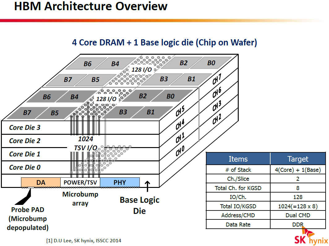
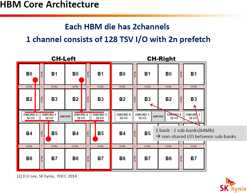
The HBM JESD235 standard stacks four DRAM dies with two 128-bit channels per die on a base logic die, which results into a memory device with a 1024-bit interface. Each channel is similar to a standard DDR interface, but is completely independent and therefore each channel within one stack and even within one die can operate at different frequency, feature different timings and so on. Each channel supports 1Gb – 32Gb capacities, features 8 or 16 banks (16 banks configuration is used with 4Gb and larger channels) and can operate at 1Gb/s – 2Gb/s data-rates (1GHz – 2GHz effective DDR frequency). As a result, each HBM 4Hi stack (4 high stack) package can provide 1GB – 32GB capacity and 128GB/s – 256GB/s memory bandwidth. It is expected that the HBM JESD235 standard will evolve to accommodate stacks of eight DRAM dies (HBM 8Hi stack package/topology).
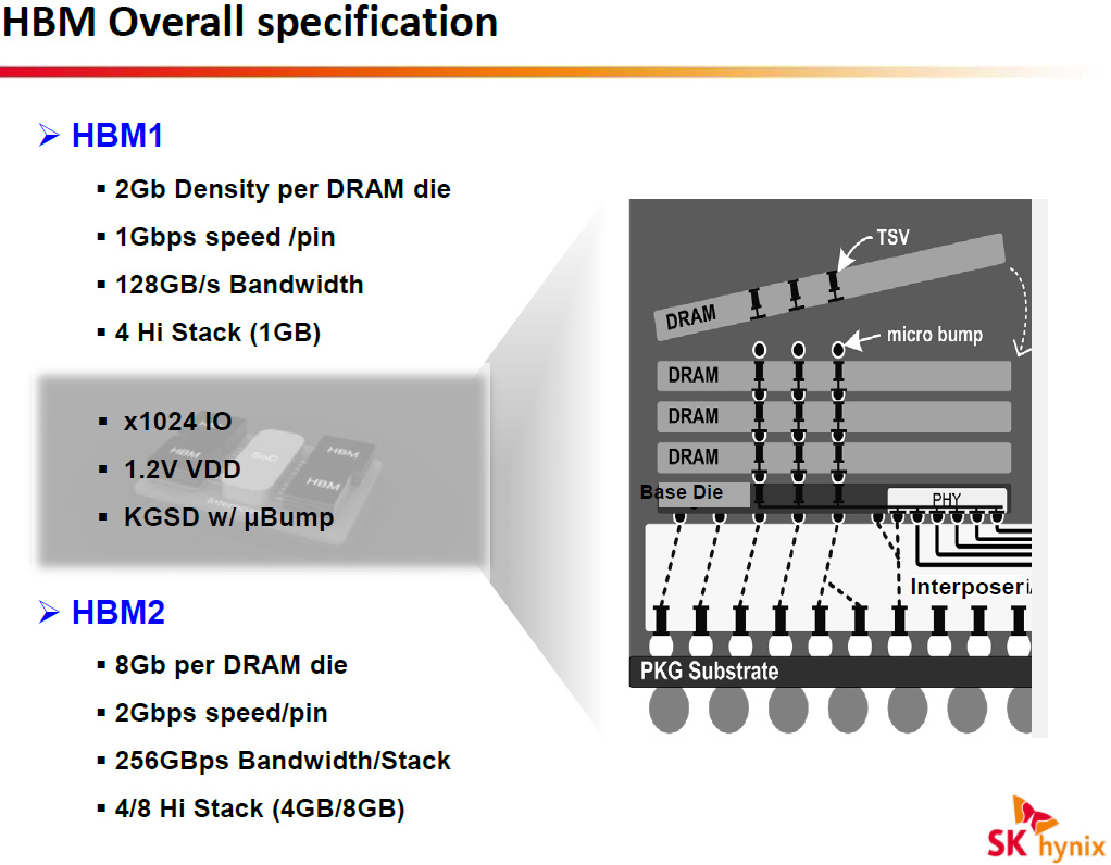
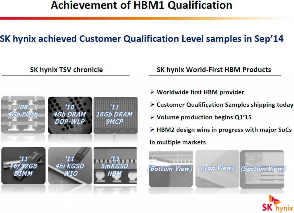
Back in September, 2014, SK Hynix started to ship its QL samples to customers for qualification purposes. The qualification level (QL) sample of SK Hynix HBM memory solution (H5VR8GESM4R-20C), which is listed in the company’s Q4 2014 databook, has 1GB density (even though the document states that the chip has 1Gb density, its H5VR8GESM4R-20C product number implies that its density is 8Gb, not 1Gb), 1024-bit wide interface and 1Gb/s per pin data-rate, which results in massive 128GB/s per-device bandwidth. The high-bandwidth memory chip uses 5mKGSD (molded known good stacked die) packaging that stacks four 2Gb dynamic random access memory dies on one base logic die. The QL 4Hi stack HBM deivce features VDD/VDDQ voltages of 1.2V. The particular 1GB HBM chip may be designed for qualification purposes and it is unknown whether it will be used for commercial products.
Recently SK Hynix announced that it would start mass production of commercial HBM DRAM devices in the first quarter of 2015. The first commercial HBM chip is expected to feature 8Gb capacity (eight 1Gb 128-bit channels, four 2Gb DRAM dies), 1024-bit wide interface, 1Gb/s per pin data-rate and 1.2V voltage. In general, all architectural, clock-rate and electrical specifications of the commercial HBM 4Hi stack are similar to those of QL samples. The chip will be made using 29nm process technology. It is possible that there will be commercial HBM chips with 1.25Gb/s data rate.
According to market rumours, AMD’s next-generation Radeon R9 390X “Fiji XT” graphics processing unit (which is expected [based on a leak in SiSoft Sandra’s database] to feature 4096 stream processors/64 compute units, 256 texture units) will feature 4096-bit memory interface to connect to four SK Hynix HBM devices. Based on the leak, the Radeon R9 390X’s memory interface operates at 1.25Gb/s data-rate (1.25GHz effective DDR frequency) and delivers whopping 640GB/s memory bandwidth. Even at “standard” 1Gb/s per-pin data-rate the memory sub-system will feature 512GB/s bandwidth.
AMD has neither confirmed nor denied plans to use SK Hynix HBM 4Hi stack DRAM devices on its next-generation graphics adapters. Nvidia Corp., another potential adopter of HBM, publicly stated that its first graphics processor to support HBM DRAM will be based on the code-named “Pascal” architecture that will be released in 2016. The fact that SK Hynix will start to manufacture appropriate devices in volume in Q1 2015 implies that there is a customer who needs HBM devices in the first half of next year.

Discuss on our Facebook page, HERE.
KitGuru Says: The evidence mounts that AMD’s next-generation high-performance graphics adapters based on the “Fiji XT” and “Fiji Pro” graphics processing units will use high-bandwidth memory (HBM) sub-systems with unprecedented bandwidth. Based on the information from SK Hynix, qualification of its HBM devices is well underway and mass production is on-track for Q1 2015. Looks like a revolution is incoming. Imagine what kind of performance will a GPU with 4096 stream processors, 256 texture units and up to 640GB/s memory bandwidth provide in 4K (3840*2160) ultra-high-definition resolution! Just a small reminder: 1Gb/s data rate is just the start for the HBM memory type.

Nvidia talked about his last year before they updated their Roadmap. Volta’s marque feature will be stacked DRAM, which sees DRAM placed very close to the GPU by placing it on the same package, and connected to the GPU using through-silicon vias (TSVs). Having high bandwidth, on-package RAM is not new technology, but it is still relatively exotic.
NVIDIA is targeting a 1TB/sec bandwidth rate for Volta, which to put things in perspective is over 3x what GeForce GTX Titan currently achieves with its 384bit, 6Gbps/pin memory bus (288GB/sec). This would imply that Volta is shooting for something along the lines of a 1024bit bus operating at 8Gbps/pin, or possibly an even larger 2048bit bus operating at 4Gbps/pin. Volta s still years off, but this at least gives us an idea of what NVIDIA needs to achieve to hit their 1TB/sec target.
This is what was said over a year ago, but this time around it’s with Pascal instead of Votla or you could possibly say it’s the best of two worlds in Pascal. http://blogs.nvidia.com/blog/2014/03/25/gpu-roadmap-pascal/
PhoneyVirus
https://twitter.com/PhoneyVirus
https://phoneyvirus.wordpress.com/
AMD doing HBM at 2015 whereas nVidia doing HBM at 2016. nVidia is too late
Nvidia is going to be using HBM from SK Hynix in Pascal. They may eventually use their HCM type if they can actually get it relatively back on track for the roadmap. Right now it’s way too far behind to be used any time in the next 2 years. Also, the second iteration of HBM is going to have double the bandwidth available, by doubling the speed each pin can run at, so for cards released in 2016, 2048-bit bus = 512GB/s and 4096-bit bus = 1TB/s. Also every stack has 1024-bit I/O, and I seriously doubt Nvidia plans on limiting all of their cards to 2GB and 4GB configurations. I would hope they plan on using 4GB and 8GB variations of cards using a 4096-bit bus.