

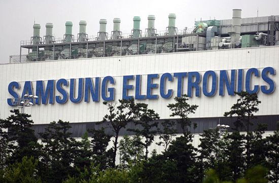
Samsung Electronics plans to invest additional $9.2 billion in capacity expansion of the world’s largest semiconductor fab, a media report claims. At present it is unclear how exactly Samsung plans to expand its fab, but the cost of the whole project – around $23.6 billion – already looks staggering.
Samsung announced plans to build its gigantic semiconductor manufacturing facility near Pyeongtaek, South Korea, last October. The fab is expected to be twice as wide as Samsung’s S1 plant in Giheung, South Korea, and can accommodate up to five semiconductor production lines, it was revealed earlier this month. The production facility is expected to be used primarily for DRAM [dynamic random access memory]. The plant requires investment of 15.6 trillion won ($14.4 billion) and is set to begin operations in 2017.
Even though exact production capacity of the fab remains unknown, keeping in mind that it is bigger than Samsung’s S1 semiconductor fabrication plant, which can process 170 thousand of 300mm wafers a month, it is likely that the new fab will be the world’s first plant with capacity of at least 300 thousand 300mm wafer starts per month.
Samsung is not standing still. Reuters news-agency reports that the company is already mulling capacity expansion investment plan for the semiconductor fab. At this time, the company is expected to spend at least another 10 trillion won ($9.2 billion) to boost capacity at its new manufacturing facility. The report does not reveal when the additional investment is set to take place.
At present it is unclear how exactly Samsung plans to increase production capacity of its fab near Pyeongtaek, South Korea, but there are at least three options:
- Increase the amount of production lines by physically expanding the fab.
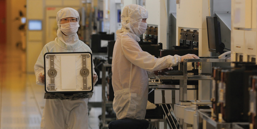
- Install extreme ultraviolet (EUV) lithography equipment in existing fab. This could improve yield and lower complexity of manufacturing operations, which could ultimately lead to increase of wafer starts per month and production capacity. EUV equipment will be used for DRAM production one or two years after companies start to use it for production of advanced chips like microprocessors, according to ASML. Since EUV is not going to be used until at least 2017, DRAM will be produced using the new lithography tools only in 2019-2020 at the earliest.
- Convert the fab to 450mm wafers and effectively increase its chip output by 2.25 times. While this plan brings the most benefits, 450mm equipment is not going to be ready for mass production for years. Moreover, transition to 450mm equipment is a risky one in general.
Samsung did not comment on the news-story.
Discuss on our Facebook page, HERE.
KitGuru Says: Since the information comes from an unofficial source, it may not be accurate. In fact, Samsung could spend $9.2 billion over many years just to install new equipment as it transits to thinner manufacturing technologies. Since this process inevitably involves installation of EUV scanners, it also could lead to increase of wafer starts per month.

< col Hiiiiiii Friends….'my friend's mom makes $88 every hour on the internet . She has been unemployed for eight months but last month her payment was $13904 just working on the internet for a few hours.
try this site HERE’S MORE DETAIL
????????tuy
< ??????? Hiiiiiii Friends….'s step-aunt makes $61 an hour on the computer. She has been out of work for five months but last month her paycheck was $19373 just working on the computer for a few hours. see this site= HERE’S MORE DETAIL
۩۞۩ஜ▬▬▬▬▬▬▬▬▬▬▬▬▬ஜ۩۞۩ஜ۩۞۩ஜ▬▬▬▬▬▬▬▬▬▬▬▬▬ஜ۩۞۩ஜ
††††††††††dfer
DRAM? Which is outdated at this point we need something like…HBM…?