

Toshiba Corp. on Wednesday said it would demolish one of its fabs in Yokkaichi, the company's NAND Flash memory manufacturing complex in Mie prefecture, Japan, and build an all new factory specially to produce 3D NAND flash. The new fab is expected to be complete next Summer and will go online in 2016. Toshiba and its partner SanDisk Corp. also signed a memorandum of understanding regarding joint investment into the new fab.
The new wafer fab will be primarily used to secure space for converting existing Toshiba and SanDisk 2D NAND capacity to 3D NAND beginning in 2016. The factory will provide an additional facility for processes designed for 3D NAND memory production, and work in close collaboration with Yokkaichi's other facilities. Toshiba and SanDisk will support 3D memory production with leading-edge manufacturing equipment for lithography, deposition and etching through joint ventures.
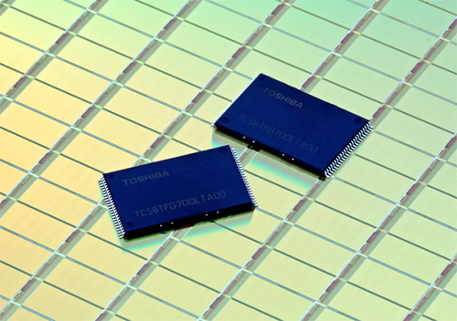
3D NAND or Vertical NAND (V-NAND) memory stacks memory cells vertically and uses a charge trap flash architecture. The vertical layers allow larger areal bit densities without requiring smaller individual cells, which means higher reliability and performance. In the coming years it will become harder for NAND flash makers to continue scaling process technologies and make them thinner, which is when 3D NAND will come into play. Flash producers who want to stay relevant in the coming years are naturally getting ready to make 3D NAND in mass quantities. Samsung recently started to produce 3D NAND at its brand-new fab in China.
Demolition work on the current fab 2 will begin in May, the construction of the new fab is set to start in September 2014. The company plans to complete the building in the Summer of 2015.
The clean room within the new fab will be built in phases to align the clean room investment with the timing of conversion of 2D NAND capacity to 3D NAND. Construction of the initial cleanroom will be complete in time for 2016 output. Decisions on capacity conversion ramp and equipment investment, the start of production, and production levels in the new fab will reflect market trends, Toshiba indicated.
The new fab will have a quake absorbing structure and an environmentally friendly design that includes LED lighting throughout the building.
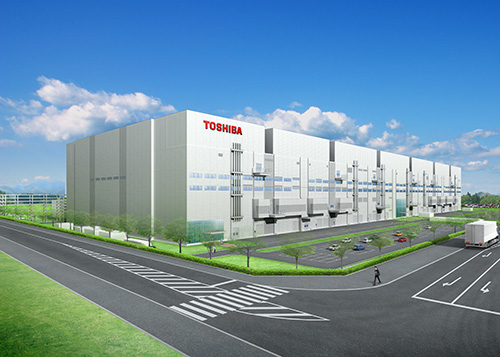
Toshiba’s Yokkaichi operations consist of multiple wafer fabs. The fab 1 started to manufacture semiconductors in 1992. The fab 2, which is set to be demolished, became operative in 1995. At present Yokkaichi complex includes five advanced memory manufacturing plants many of which are state-of-the-art.
Discuss on our Facebook page, HERE.
KitGuru Says: It is remarkable that Toshiba will demolish a fab and build a new one while not ceasing operations of other factories in the complex completely. Since modern semiconductor facilities use extremely thin – 19nm or 25nm – manufacturing technologies any shock may harm production and there will be plenty of shocks here and there during demolition and construction. Looks like Toshiba is confident about shock absorbing capabilities of its other fabs in Yokkaichi.