

GlobalFoundries is working on its own 7nm and 10nm fabrication processes and it does not look like the company has plans to license technologies from the outside. The contract maker of semiconductors hopes that specialists from IBM’s microelectronics unit will help it to design world-class leading-edge manufacturing processes.
GlobalFoundries, which was once manufacturing arm of Advanced Micro Devices, used to have problems with delivering advanced manufacturing technologies on time. Over the years, GlobalFoundries’ management did a lot to add competitive advantages to the company: it acquired Chartered Semiconductor, brought-in a lot of talent from the outside and participated in various industry-wide initiatives. While it did help to make GlobalFoundries the world’s No. 2 or No. 3 contract maker of chips, the company struggled to remain competitive with its leading-edge technologies, a hard thing to do nowadays.
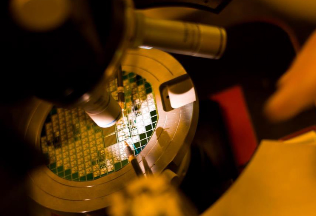
The company had issues with its 32nm SOI process technology, it was late with 28nm node, it cancelled 28nm FDSOI and it was going to be late-to-market with its 14nm-XM process. In a bid to catch up and potentially gain new customers, GlobalFoundries licensed 14nm LPE [low-power early] and 14nm LPP [low-power plus] technologies from Samsung Electronics. However, going forward GlobalFoundries hopes to develop its own manufacturing processes. The combined team of IBM and GF engineers is expected to deliver robust 10nm and 7nm fabrication technologies.
“We are developing our own technologies for the next nodes,” said Sanjay Jha, chief executive officer of GlobalFoundries, in an interview with EETimes web-site. “The whole point of the IBM Microelectronics business acquisition is to leverage IBM’s technologists and technology to accelerate our own development of leading-edge process technologies.”
Mr. Jha does not reveal any timeframes concerning 10nm fabrication process and any kind of targets that the company wants to hit with the manufacturing technology. Keeping in mind that Samsung Electronics and Taiwan Semiconductor Manufacturing Co. plan to start production of chips using their 10nm processes in late 2016 or early 2017, it is obvious that GlobalFoundries will be behind its rivals. In a bid to start low-volume production using 10nm manufacturing tech in late 2016 or early 2017, GF needed to deliver early process design kits (PDKs) to its customers three to six months ago. The technology is in development and no PDKs are available to key clients like Advanced Micro Devices.
Mr. Jha is confident that extreme ultraviolet (EUV) lithography will not be commercially viable before 2018 or 2019, which is in line with expectations by other industry executives.
“We are not expecting EUV before 2018 or 2019,” said Mr. Jha. “We are focused on optical tools for 10nm and 7nm. As EUV stabilizes, we may use EUV for some layers. We are also using EUV to accelerate prototyping.”
Discuss on our Facebook page, HERE.
KitGuru Says: It is clear that GlobalFoundries will be behind its rivals with 10nm manufacturing technology. While GlobalFoundries will likely try to make its 10nm competitive in order not to let its main customer down, it is obvious that the joint team of IBM and GloFo will focus on 7nm fabrication process. Keeping in mind that IBM experimented with a number of promising technologies and that intellectual property is now available to GlobalFoundries, we can expect very interesting results. It is possible that at 7nm the foundry industry will have three viable competitors (or four, if Intel is considered a foundry). The main question is whether GlobalFoundries will have enough money to develop that state-of-the-art process technology…

This is wishful thinking that GF with IBM can develop their own 10nm forget 7.
how about AMD Zen 14nm proc ?
my associate’s stride close relative makes $98 an hour on the portable workstation……….Afterg an average of 19952 Dollars monthly,I’m finally getting 97 Dollars an hour,just working 4-5 hours daily online.….. Weekly paycheck… Bonus opportunities…earn upto $16k to $19k /a month… Just few hours of your free time, any kind of computer, elementary understanding of web and stable connection is what is required…….HERE I STARTED…look over here
—-hs.
➤➤➤➤ http://GoogleTopTrendingJobsNetworkOnlineCenters/$98hourlywork…. =★★★★★★★★★★★★★★★★★★★★★★★★★★★★★★★★★★
As stated in the article, they licensed the 14nm techs from Samsung
Really? IBM was the only foundry in the world that could keep pace with Intel, not to mention IBM’s already demo’ed working 7nm silicon.
Not to be pedantic, but shouldn’t the headline read, “Global Foundries developing…”? Using “develops” makes it sound past tense and that the technology has already been developed.
But that IBM 7nm demo stuff was more like 10nm. We are at one weird point where node labels did loose their meaning completely.
You need to “lose” an “o” on your “loose”.
People are griping about Intel’s 14nm really not being 14nm or other’s 16nm really being 20nm. People need to chill. 7 or 10 it is still an amazing accomplishment.
You have no citable proof of that.
Seriously. Intel made about $55B in 2014 with Net Profit of $16B. IBM paid $1.5B to unload $2B/year losing semiconductor business. IBM can write the patents but has never done anything that can be manufactured. Demoing 7nm means nothing unless you can make money.
Uh, wrong eight ways from Sunday. The Power 8 series has been their most lucrative yet. The foundry was too expensive (IBM was the only customer, so it didn’t have the volume which makes Intel’s viable), not the chip design and sales. IBM’s profit margins make Intel look like a charity.
i find it hard to believe glofo managed to snag IBM tech away from the likes of TSMC, Intel, or Samsung if they had legitimate working 7nm tech . . . it just doesn’t make sense.
Either its not that great or others already have 7 and 10nm tech that is as advanced as IBMs.
It makes perfect sense. IBM is a chief rival of both Samsung and Intel. Taiwan wants to keep its foundries all in Taiwan. TSMC probably didn’t make an offer.
valid points . . . i just find it hard to believe they gave away working 10nm and 7nm technology. and glofo isnt exactly confidence inspiring.
I wouldn’t say they gave it away. What they have done is erased their foundry costs to focus on hardware and software design and delivering Infrastructure as a Service for cloud-based servers. However, as a matter of pride, IBM stuck it to Intel and Samsung with a big old one-finger salute.