

SK Hynix has demonstrated a wafer with second-generation high-bandwidth memory (HBM) at the CeBIT trade-show in Hannover, Germany. The new memory chips will emerge on the market sometimes next year and will increase memory bandwidth and memory capacities for graphics cards and other applications.
The first-generation HBM (HBM1) stacks four DRAM dies with two 128-bit channels per die on a base logic die, which results into a memory device with a 1024-bit interface. Each channel supports 1Gb capacities (2Gb per die), features 8 banks and can operate at 1Gb/s – 1.25Gb/s data-rates (1GHz – 1.25GHz effective DDR frequency). As a result, each HBM 4Hi stack (4 high stack) package can provide 1GB capacity and 128GB/s – 160GB/s memory bandwidth. The first-gen HBM stacks are made using 29nm (which SK Hynix calls “2xnm”) process technology. While even the first-generation HBM can enable graphics cards with up to 8GB (with the help of dual-link interposing) of memory and 640GB/s of bandwidth, it will not be enough for the future.
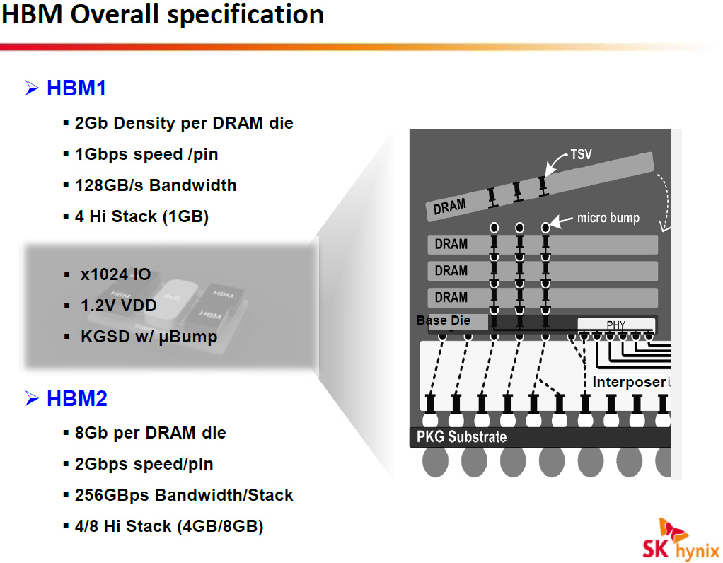
The second-generation HBM (HBM2) greatly expands capabilities of the high-bandwidth memory in general and will evolve in the coming years. The HBM2 uses 8Gb dies with two 128-bit channels featuring 16 banks. Data-rates of the second-generation HBM will increase up to 2Gb/s (2GHz effective DDR frequency). The architecture of the HBM2 will let manufacturers built not only 4Hi stack (4 high stack) packages, but also 2Hi stack and 8Hi stack devices.
In the best-case scenario HBM2 memory chips will feature 8GB capacity (8Hi stack) with 256GB/s bandwidth (2Gb/s data rate, 1024-bit bus). Such HBM2 devices will let developers of graphics processing units to build graphics adapters with 32GB of onboard memory and incredible 1TB/s peak bandwidth. Nvidia Corp. has already announced that its next-generation code-named “Pascal” graphics processing architecture will support up to 32GB of HBM2. Mainstream HBM2 ICs will likely sport 2GB (2Hi stack) or 4GB (4Hi stack) capacities with 1.6Gb/s data rate (204.8GB/s bandwidth per chip), which should be more than enough for high-performance graphics cards in 2016.
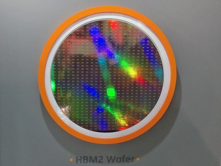
Fudzilla reports that SK Hynix demonstrates a wafer with HBM2 memory ICs [integrated circuits] at CeBIT. Typically, manufacturers of memory can show off future DRAM products years before mass production. According to a roadmap leaked by SemiAccurate some time ago, SK Hynix plans to start production of HBM 2 in early 2016. It is expected that second-gen HBM stacks will be manufactured using 20nm fabrication process (which SK Hynix calls “2znm”).
Going forward the JESD235 standard that powers HBM memory will evolve in terms of clock-rates, die densities (do not expect 16Gb dies any time soon, though) and other ways to improve performance. Extreme memory bandwidth will be required by high-end graphics cards in the coming years as the world transits to ultra-high-definition displays with 4K (3840*2160, 4096*2160) and 5K (5120*2880) resolutions. Even more memory bandwidth will be needed towards the end of the decade when the first displays with 8K (7680*4320) resolutions emerge.
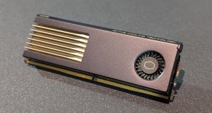
The first graphics cards to use HBM memory will be AMD’s next-generation Radeon R9 390X. The new graphics processing unit from AMD reportedly features 4096 stream processors/64 compute units, 256 texture mapping units and 4096-bit memory bus. The Radeon R9 390X’s memory interface operates at 1.25Gb/s data-rate (1.25GHz effective DDR frequency) and delivers whopping 640GB/s memory bandwidth.
Discuss on our Facebook page, HERE.
KitGuru Says: The HBM looks incredibly good on paper. It provides nice scaling both in terms of bandwidth and capacity for devices like graphics cards. Nonetheless, it is obvious that HBM is not cheap and will never become a standard for system memory.
Finally something that scream progress
HBM 2 based AMD APU’s would be awesome. GTX 750Ti or R7-260X like performance on an APU !! With 14nm node performance of APUs with HBM tech may even touch R9 270X performance easily.
The problem you’re not considering is the fact that these APU’s lack the necessary hardware outside of faster and more expansive DDR. This is only a slice of the pie. Stream processors, ROPs, core speeds, heat dissipation, power usage and so much more factors into the ability to make an APU even close to mid-level graphics.
I would estimate R7-250X performance at best… Still, not bad all things considered… spending $200 on more and better RAM.. vs getting cheaper RAM and just getting a dedicated card which will always be better than an APU… and function better in tandem.
Pls enlightened me, with 8 hi stack should the speed be multiplied by 8 as well? If each die feature 128×2 bits den 8 hi stack would correspond to 2048 bits?
Also it mentioned 8Gb capacity but is dual 2Gb = 4Gb? So is 8 or 4 Gb? In any case I felt it would be 8GB at 512GB/s for a 8 hi stack die.
In any case I want to know what is the different between 4 hi stack and 8-hi stack, the capacity will doubled, but the Bandwidth double also? The number just don’t make sense.
“Nonetheless, it is obvious that HBM is not cheap and will never become a standard for system memory.”
AMD has Patents that clearly are going in that direction. Taking the DRAM socket and packaging cost out of the picture never mind a 50% smaller MOBO will likely pay for any increase in cost that HBM interposer stacked system DRAM will cause.
Not to mention the increase in performance that comes from eliminating the electrical path latency from the the equation.
HBM will be on Zen APU’s too. Likely as another level of cache but also for increased APU performance as well.
HBM 2 or 3 replacing system DRAM is the 1600# gorilla in the room.
If AMD can put 4-8 gigs of HBM on a GPU then they can do the
same with CPU’s as well as APU’s. In fact one interesting quote from the
patents listed below is this:
“Packaging chips in closer proximity not only improves
performance, but can also reduce the energy expended when communicating between
the processor and memory. It would be desirable to utilize the large amount of
“empty” silicon that is available in an interposer.”
AMD has plans to fill that empty silicon with much more memory.
The point: REPLACE SYSTEM DYNAMIC RAM WITH ON-DIE HBM 2 OR 3!
Eliminating the electrical path distance to a few millimeters from 4-8
centimeters would be worth a couple of clocks of latency. If AMD is building
HBM and HBM 2 then they are also building HBM 3 or more!
Imagine what 64gb of HBM could do for a massive server die such
as Zen? The energy savings alone would be worth it never mind the hugely
reduced motherboard size, eliminating sockets and RAM packaging. The increased
amount of CPU’s/blade or mobo also reduces costs as servers can become much
more dense.
Most folks now only run 4-8 gigs in their laptops or desktops.
Eliminating DRAM and replacing it with HBM is a huge energy and mechanical
savings as well as a staggering performance jump and it destroys DDR5. That
process will be very mature in a year and costs will drop. Right now the retail
cost of DRAM per GB is about $10. Subtract packaging and channel costs and that
drops to $5 or less. Adding 4-8 GB of HBM has a very cheap material cost,
likely the main expense is the process, testing and yields. Balance that
against the energy savings MOBO real estate savings and HBM replacing system
DRAM becomes even more likely without the massive leap in performance as an
added benefit.
The physical cost savings is quite likely equivalent to the
added process cost. Since Fiji will likely be released at a very competitive
price point.
AMD is planning on replacing system DRAM memory with stacked
HBM. Here are the Patents. They are all published last year and this year with
the same inventor; Gabriel H. Loh and the assignee is of course AMD.
Stacked memory device with metadata management
WO 2014025676 A1
“Memory bandwidth and latency are significant performance
bottlenecks in many processing systems. These performance factors may be
improved to a degree through the use of stacked, or three-dimensional (3D),
memory, which provides increased bandwidth and reduced intra-device latency
through the use of through-silicon vias (TSVs) to interconnect multiple stacked
layers of memory. However, system memory and other large-scale memory typically
are implemented as separate from the other components of the system. A system
implementing 3D stacked memory therefore can continue to be bandwidth-limited
due to the bandwidth of the interconnect connecting the 3D stacked memory to
the other components and latency-limited due to the propagation delay of the
signaling traversing the relatively-long interconnect and the handshaking
process needed to conduct such signaling. The inter-device bandwidth and
inter-device latency have a particular impact on processing
efficiency and power consumption of the system when a performed task requires
multiple accesses to the 3D stacked memory as each access requires a
back-and-forth communication between the 3D stacked memory and thus the
inter-device bandwidth and latency penalties are incurred twice for each
access.”
Interposer having embedded memory controller circuitry
US 20140089609 A1
” For high-performance computing systems, it is desirable
for the processor and memory modules to be located within close proximity for
faster communication (high bandwidth). Packaging chips in closer proximity not
only improves performance, but can also reduce the energy expended when
communicating between the processor and memory. It would be desirable to
utilize the large amount of “empty” silicon that is available in an
interposer. ”
Die-stacked memory device with reconfigurable logic
US 8922243 B2
“Memory system performance enhancements conventionally are
implemented in hard-coded silicon in system components separate from the
memory, such as in processor dies and chipset dies. This hard-coded approach
limits system flexibility as the implementation of additional or different
memory performance features requires redesigning the logic, which design costs
and production costs, as well as limits the broad mass-market appeal of the
resulting component. Some system designers attempt to introduce flexibility
into processing systems by incorporating a separate reconfigurable chip (e.g.,
a commercially-available FPGA) in the system design. However, this approach
increases the cost, complexity, and size of the system as the system-level
design must accommodate for the additional chip. Moreover, this approach relies
on the board-level or system-level links to the memory, and thus the separate
reconfigurable chip’s access to the memory may be limited by the
bandwidth available on these links.”
Hybrid cache
US 20140181387 A1
“Die-stacking technology enables multiple layers of Dynamic
Random Access Memory (DRAM) to be integrated with single or multicore
processors. Die-stacking technologies provide a way to tightly integrate
multiple disparate silicon die with high-bandwidth, low-latency interconnects.
The implementation could involve vertical stacking as illustrated in FIG. 1A,
in which a plurality of DRAM layers 100 are stacked above a multicore processor
102. Alternately, as illustrated in FIG. 1B, a horizontal stacking of the DRAM
100 and the processor 102 can be achieved on an interposer 104. In either case
the processor 102 (or each core thereof) is provided with a high bandwidth,
low-latency path to the stacked memory 100.
Computer systems typically include a processing unit, a main
memory and one or more cache memories. A cache memory is a high-speed memory
that acts as a buffer between the processor and the main memory. Although
smaller than the main memory, the cache memory typically has appreciably faster
access time than the main memory. Memory subsystem performance can be increased
by storing the most commonly used data in smaller but faster cache
memories.”
Partitionable data bus
US 20150026511 A1
“Die-stacked memory devices can be combined with one or
more processing units (e.g., Central Processing Units (CPUs), Graphics
Processing Units (GPUs), and Accelerated Processing Units (APUs)) in the same
electronics package. A characteristic of this type of package is that it can
include, for example, over 1000 data connections (e.g., pins) between the one
or more processing units and the die-stacked memory device. This high number of
data connections is significantly greater than data connections associated with
off-chip memory devices, which typically have 32 or 64 data connections.”
Non-uniform memory-aware cache management
US 20120311269 A1
“Computer systems may include different instances and/or
kinds of main memory storage with different performance characteristics. For
example, a given microprocessor may be able to access memory that is integrated
directly on top of the processor (e.g., 3D stacked memory integration),
interposer-based integrated memory, multi-chip module (MCM) memory,
conventional main memory on a motherboard, and/or other types of memory. In
different systems, such system memories may be connected directly to a
processing chip, associated with other chips in a multi-socket system, and/or
coupled to the processor in other configurations.
Because different memories may be implemented with different
technologies and/or in different places in the system, a given processor may
experience different performance characteristics (e.g., latency, bandwidth,
power consumption, etc.) when accessing different memories. For example, a
processor may be able to access a portion of memory that is integrated onto
that processor using stacked dynamic random access memory (DRAM) technology
with less latency and/or more bandwidth than it may a different portion of
memory that is located off-chip (e.g., on the motherboard). As used herein, a
performance characteristic refers to any observable performance measure of
executing a memory access operation.”
“NoC Architectures for Silicon Interposer Systems Why pay
for more wires when you can get them (from your interposer) for free?” Natalie
Enright Jerger, Ajaykumar Kannan, Zimo Li Edward S. Rogers Department of
Electrical and Computer Engineering University of Toronto Gabriel H. Loh AMD
Research Advanced Micro Devices, Inc”
http://www.eecg.toronto.edu/~enright/micro14-interposer.pdf
“3D-Stacked Memory Architectures for Multi-Core
Processors” Gabriel H. Loh Georgia Institute of Technology College of
Computing”
http://ag-rs-www.informatik.uni-kl.de/publications/data/Loh08.pdf
“Efficiently Enabling Conventional Block Sizes for Very
Large Die-stacked DRAM Caches” Gabriel H. Loh⋆ Mark D. Hill†⋆
⋆
AMD Research † Department of Computer Sciences Advanced Micro Devices, Inc.
University of Wisconsin – Madison”
http://research.cs.wisc.edu/multifacet/papers/micro11_missmap.pdf
Energy-efficient GPU Design with Reconfigurable
In-package Graphics Memory
http://www.cse.psu.edu/~juz138/files/islped209-zhao.pdf
Unison Cache: A Scalable and Effective Die-Stacked
DRAM Cache
http://parsa.epfl.ch/~jevdjic/papers/MICRO14_unison.pdf
“This paper introduces Unison Cache, a practical and
scalable stacked DRAM cache design, which brings together
the best traits of the state-of-the-art block- and page-based
designs. Unison Cache achieves high hit rates and low
DRAM cache access latency, while eliminating impractically
large on-chip tag arrays by embedding the tags in the DRAM
cache. Cycle-level simulations of scale-out server platforms
using Unison Cache show a 14% performance improvement
over the state-of-the-art block-based DRAM cache design,
stemming from the high hit rates achieved by Unison Cache.
Unlike prior page-based designs, Unison Cache requires no
dedicated SRAM-based tag storage, enabling scalability to
multi-gigabyte stacked DRAM cache sizes.”
All of this adds up to HBM being placed on-die as a replacement
of or maybe supplement to system memory. But why have system DRAM if you can
build much wider bandwidth memory closer to the CPU on-die? Unless of course
you build socketed HBM DRAM and a completely new system memory bus to feed it.
Replacing system DRAM memory with on-die HBM has the same
benefits for the performance and energy demand of the system as it has for
GPU’s. Also it makes for smaller motherboards, no memory sockets and no memory
packaging.
Of course
this is all speculation. But it also makes sense.
This response maybe 10 months too late for you but here it is for what it is worth. Your thinking is correct and intuitively expected. However the press has done a terrible job at explaining HBM’s finer points. I don’t think I can be too hard on them because the JESD235A document isn’t very interesting to most who aren’t in the business of designing IPs around HBM, meaning design and verification engineers.
I will try to keep it short as possible and address them point by point.
1) The channels, 2 per die, implies 128 bit x 2, so under the µbump you would expect atleast 256 I/O lanes, stack them upto to 4Hi and you have 1024 I/O lanes to cater to. This is what people understood for HBM1. For HBM2, the I/O width remains 1024bits for 4Hi and 8Hi. Confusing? Yes. But here is the fine print they all missed: the logic die controls how the channels are distributed among the multiple dies. The dies are spec’d to handle 1, 2 or even 4 channels per die but in a 8Hi stack only one channel can be given to a die. This means 8 dies stacked and 8 channels of 128 bits each = 1024 bits wide I/O. In a 4Hi stack that is still 8 channels of 128 bits each but here two channels are being given per die. You can give 4 channels to a die if you wish it to be just a 2Hi stack and still have 1024 Bits. Channels can be distributed as the vendor pleases as long as the latency in all access for that particular channel remains the same. This also means two different channels can have different latencies while operating. They are not synchronous either.
2) Right now HBM1 is being made with 2Gb or 256MB dies, so 4Hi yields 8Gb or 1GB per stack in total, put 4 of those stacks to get 4GB VRAM. HBM2 expects per die capacity to go upto 8Gb or 1GB per die allowing for 4Hi stack to be 4GB, have 4 such stacks and you get 16GB of VRAM. Of course other permissible combinations also exist as you can see. Currently Hynix is using 29nm process for their HBM dies, they are going to use 21nm process for their HBM2 dies while Samsung is going to use their 20nm process for their HBM2 dies. The process tech improvements are responsible for the sizable per die capacity jump.
3) HBM2 Bandwidth is increasing because of clock speed increase with smaller process tech, but bandwidth efficiency is also increasing, due to the fact that the gaps in Activation is reduced with the 1KB page size down from 2KB page size of HBM1, this is done to deal with the tFAW 4 activation limits as per spec,for HBM1 that was 2KB * 4 = 8KB over say ~30ns clock period, there was a gap of 10ns that is being underutilized because 4 activation happened in under ~20ns, make the page size smaller to 1KB and spread it to 8 activations (tEAW) and the power consumption is kept in check plus the clock period is not wasted, this leads to better utilization of available clock period. tFAW to tEAW changes and page size reduction are just a part of the number of changes done to the modes of operation HBM can do, HBM1 was restricted to legacy mode but HBM2 is approved for pseudo channel mode as well and these changes I mentioned are part of this Pseudo Channel mode. This is mainly a power optimization thing apart from dealing with errors in the stream that can happen too frequently if the memory controllers are not upto the task. The bandwidth efficiency is really upto the PHY maker. AMD has done an outstanding job with their Fiji HBM PHYs
4) So in summary we can see the width remains the same at 1024 bits per stack be it 2,4 or 8Hi, the choice on how to implement it is upto the vendor. Bandwidth increases are primary down to clock speed increase from smaller processes 29nm to ~21/20 nm and in part to the page size being reduced and activation doubles per tEAW over from tFAW
If there are more clarifications you seek I am happy to answer them.