With the first AMD RDNA 3 products coming out in a month, AMD thought it was time to share more about the upcoming GPU architecture. That includes details about its chiplet design, physical structure, improved ray tracing and computing capabilities.
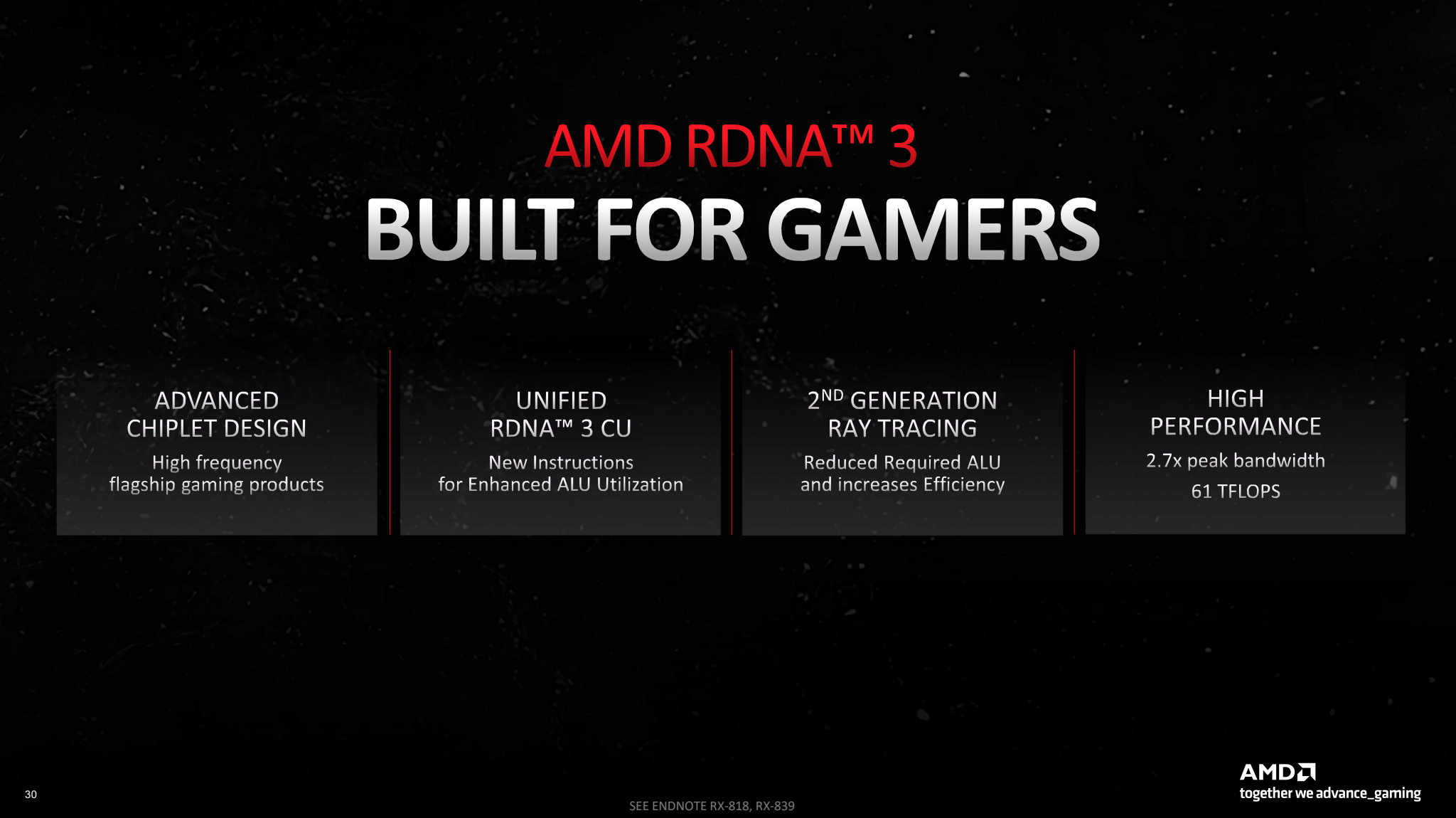
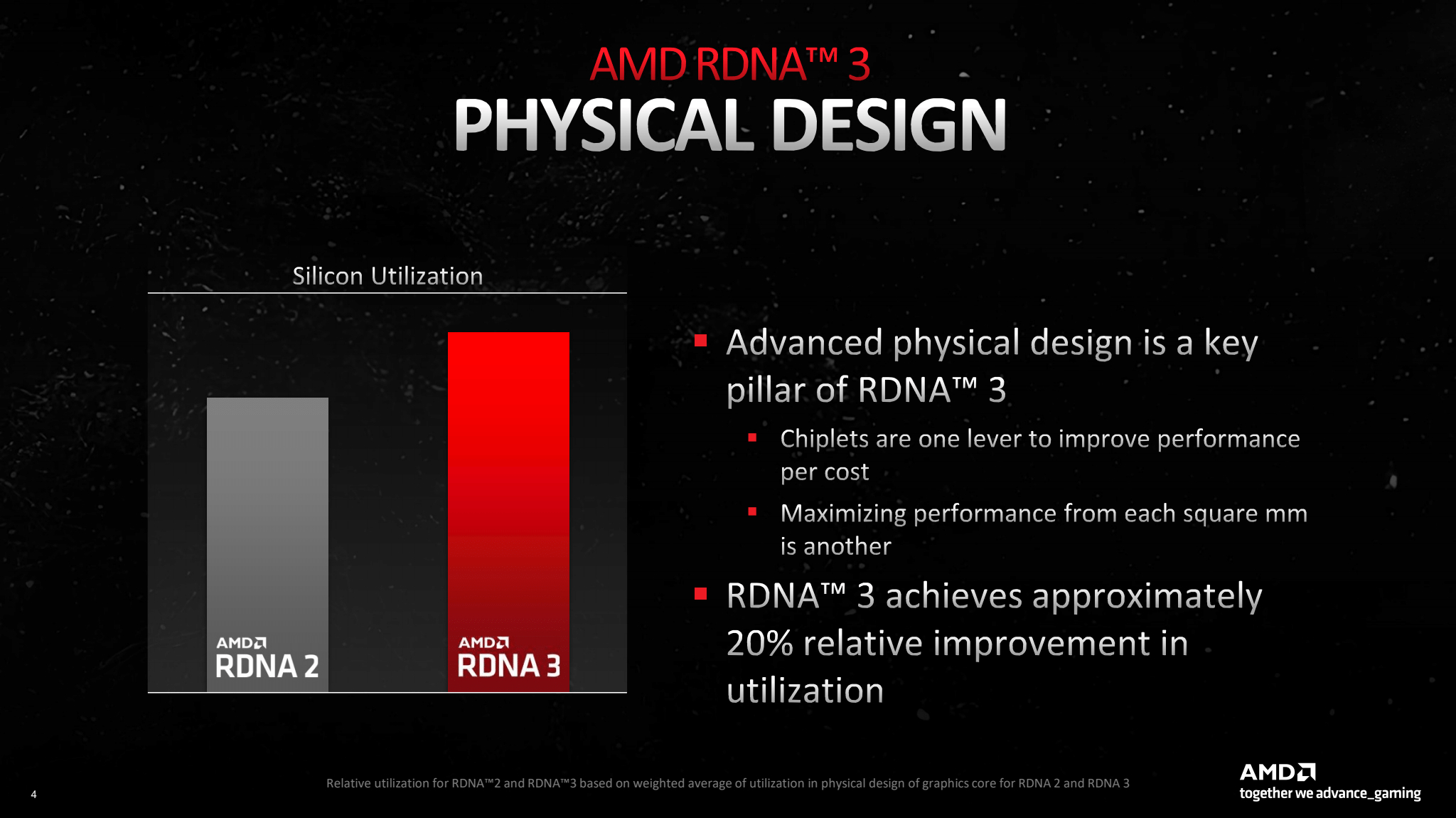
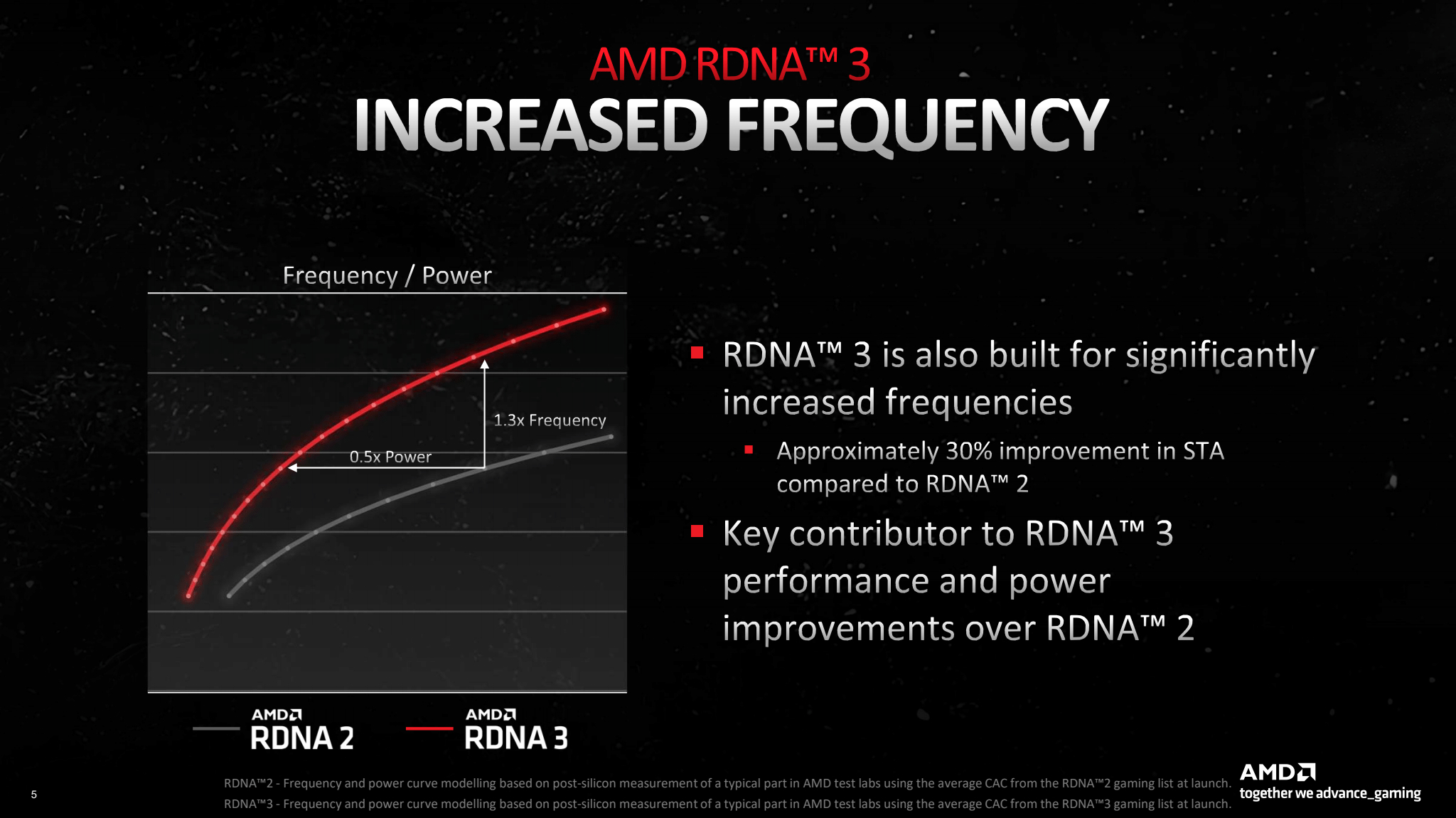
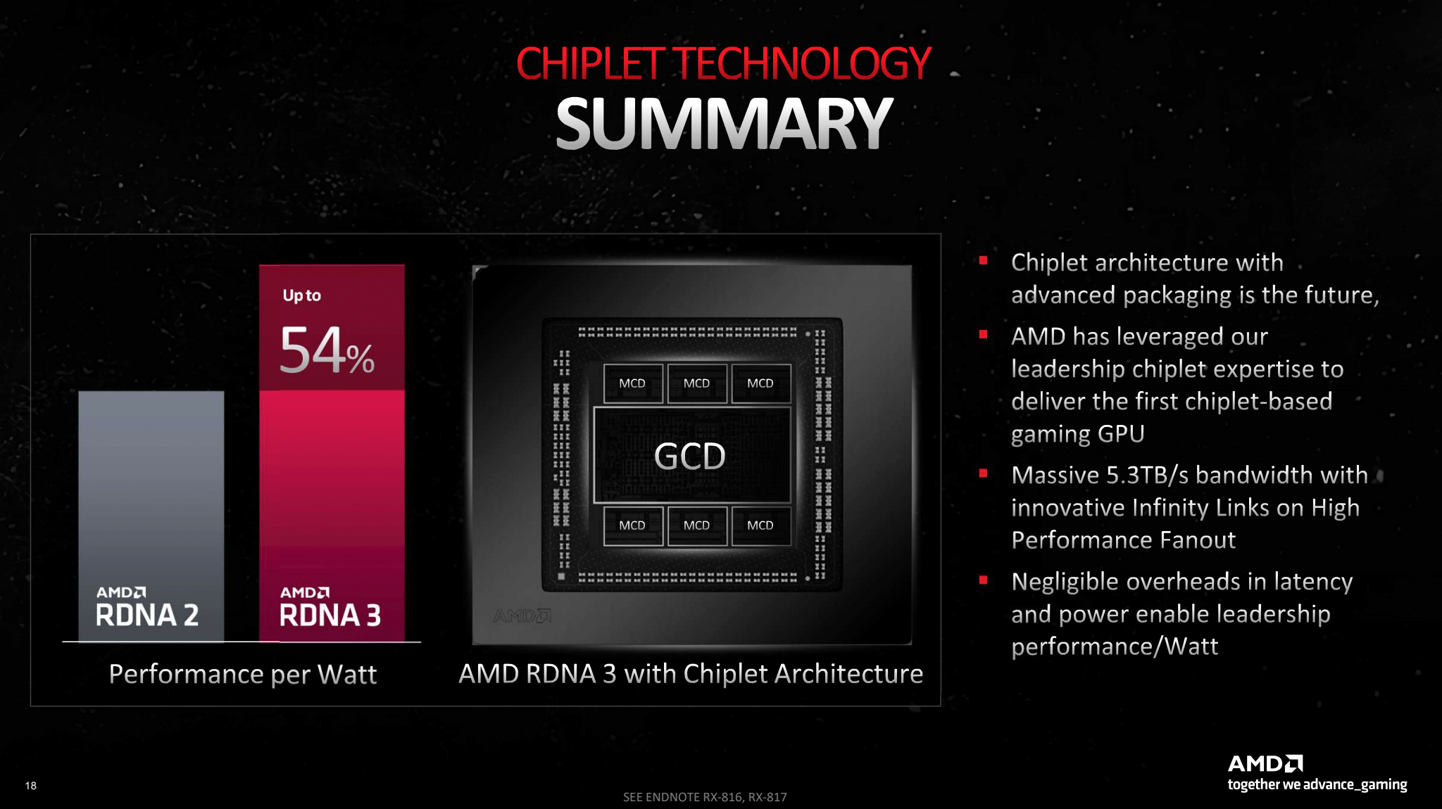
Starting with the physical design, AMD decided to go with a chiplet design instead of a monolithic one for the RDNA 3 architecture. AMD says this allowed it to improve cost to performance and maximise performance from each square mm. In the end, that results in a 20% relative improvement in silicon utilisation. The new design approach also lets the chip run faster at the same power or consume less at the same clock speed.
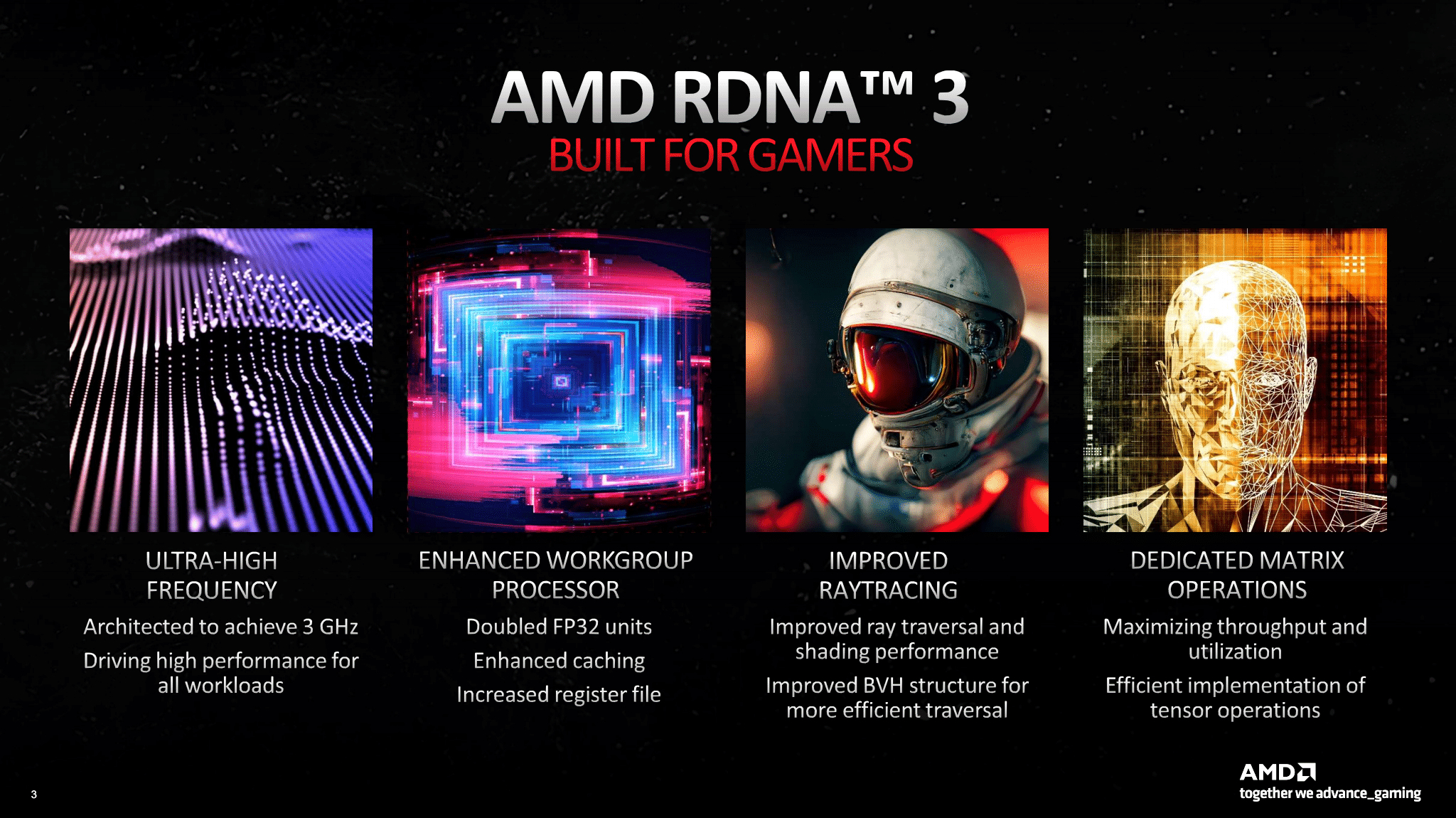
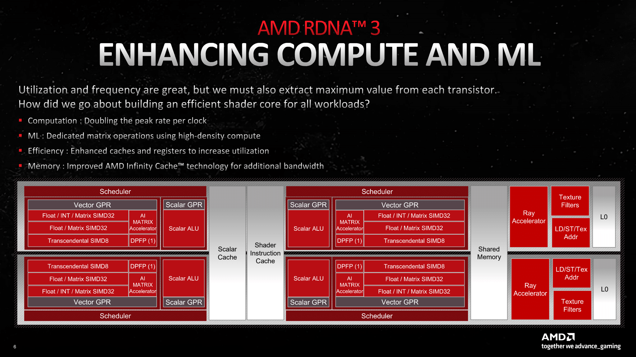
AMD had to change its current GPU architecture to build an efficient shader core for all workloads. In computation, the peak rate per clock was doubled, and in ML, dedicated matrix operations using high-density computing help to improve performance in more specific workloads. In addition, enhanced cache and registers increase silicon utilisation and improve efficiency. Lastly, the memory subsystem now offers more bandwidth thanks to the redesigned AMD Infinity Cache featured in the GPUs.
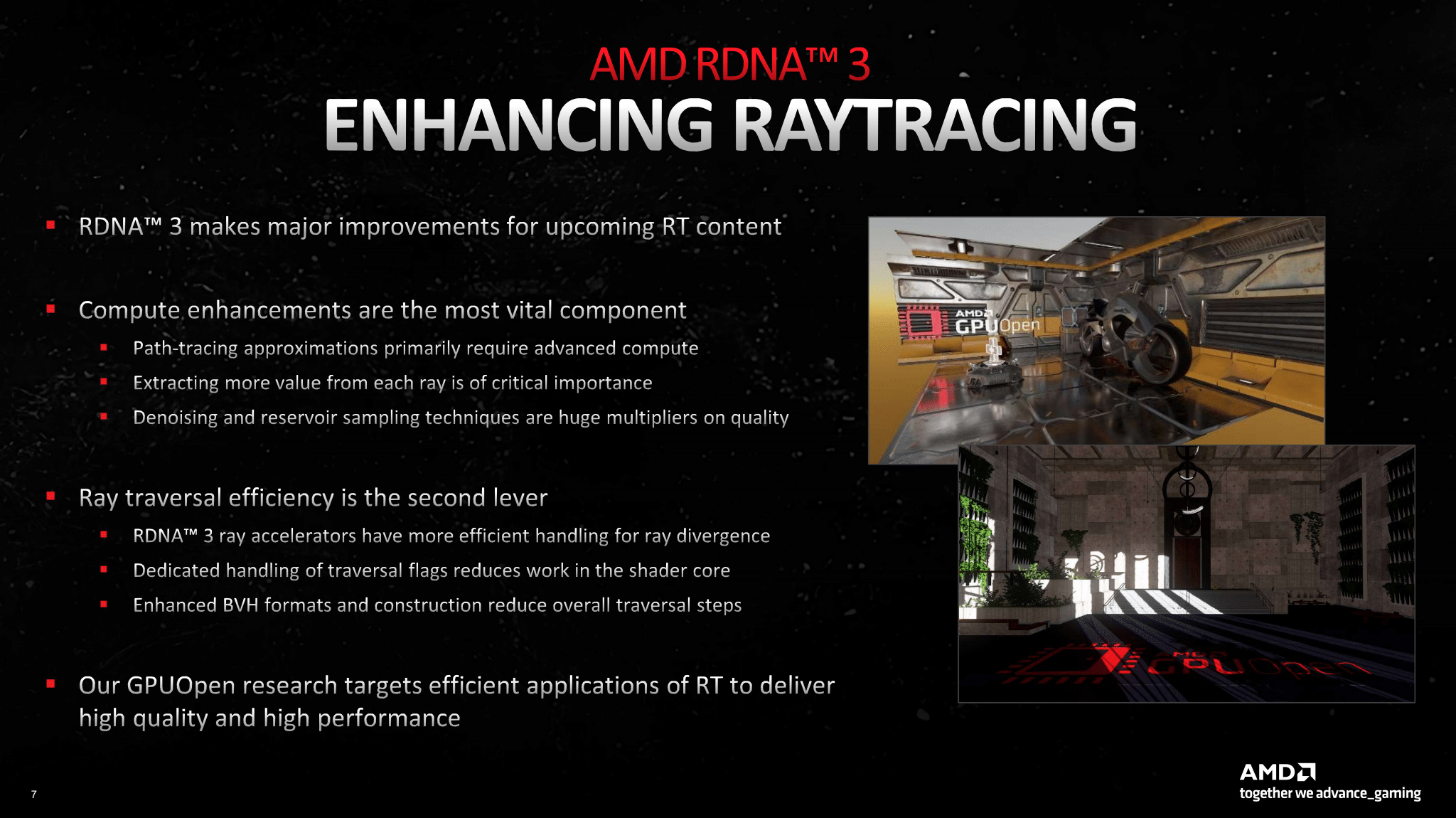
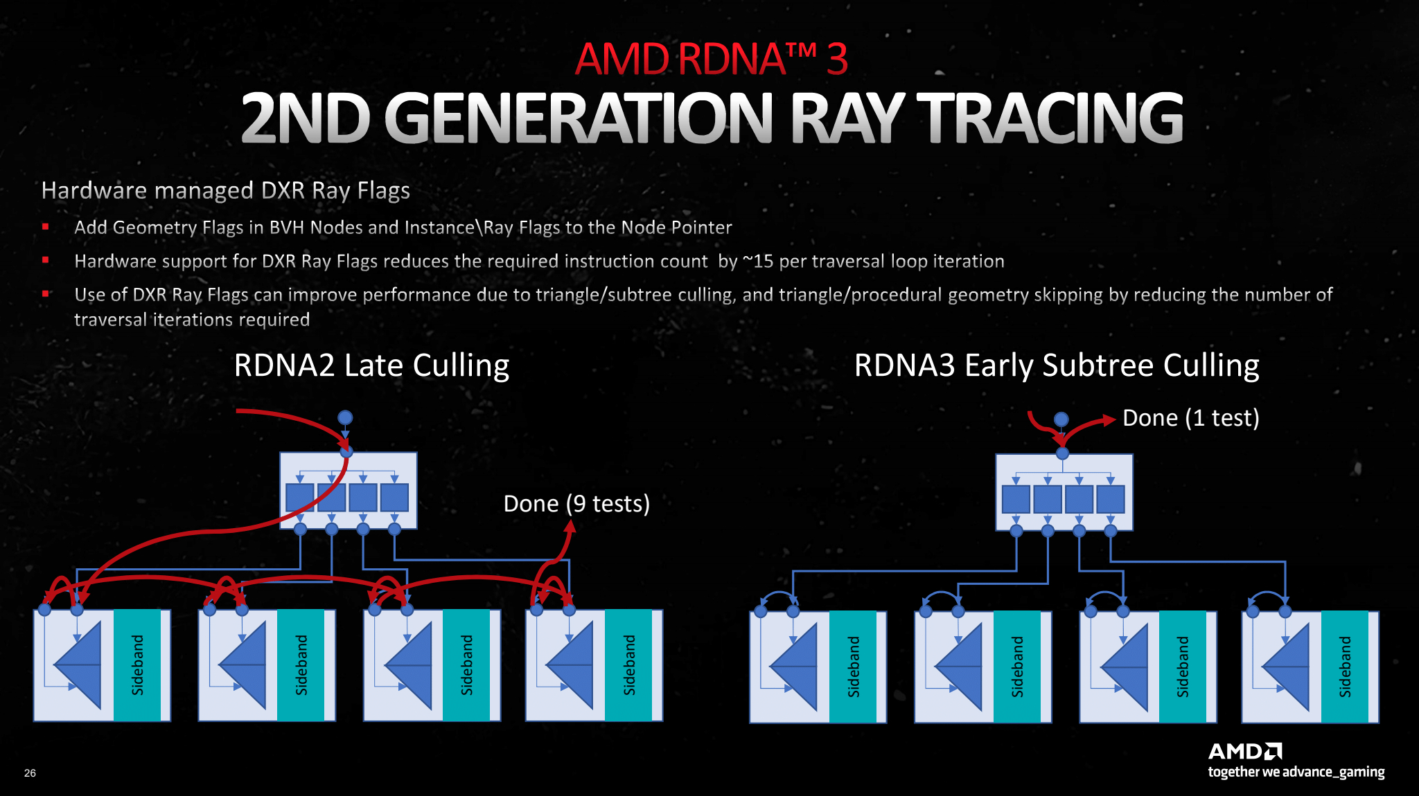
Another considerable upgrade is the ray tracing capabilities of the new GPUs. Thanks to the 2nd gen ray tracing hardware employed by AMD on the new cards, they could extract more value from each ray, improve path tracing, and use new denoising and reservoir sampling techniques. Ray transversal efficiency was also improved thanks to the new RDNA 3 ray accelerators that can better handle ray divergence and traversal flags, and reduce overall traversal steps.
AMD is already using a chiplet design on the Ryzen chips, which has seen great success. Now, AMD is bringing this over to GPUs too. There are two reasons behind this decision: diminishing returns that come with higher transistor density and increasing costs per yielded mm².
Instead, of a monolithic design, AMD separated the GFx core and upgraded it to N5. In contrast, the memory interfaces and AMD Infinity Cache controller will stay in a separate die in a more mature node. That way, the chip can benefit from the N5 performance bump at a fraction of the cost.
The chips are divided into one GCD (Graphics Compute Die) and up to six MCDs (Memory Cache Dies) with high bandwidth requirements. To solve this situation, AMD will use what it calls Infinity Fanout links, which operate at 9.2Gb/s and offer a peak bandwidth of 5.3TB/s. These links are engineered to run at a low voltage, saving up to 80% power per bit compared to organic package links. Unfortunately, they have higher latency than building the MCDs on-die, but that can be compensated for with higher Infinity Fabric and GPU clock speeds.
Another interesting bit of information shared by AMD was how the Vector units work. Due to how it's programmed, they can work as either a SIMD64 or two SIMD32 (dual-queue). Regardless of the mode, instructions still have the same clock issue and dependency rules of RDNA architectures. Moreover, the vector units can work as matrix accelerators for ray tracing and other workloads.
Discuss on our Facebook page, HERE.
KitGuru says: All of this sound very promising, but in the end, the most important thing is how all these improvements translate into real-world performance. We'll be able to take a closer look at that once reviews start coming in.