

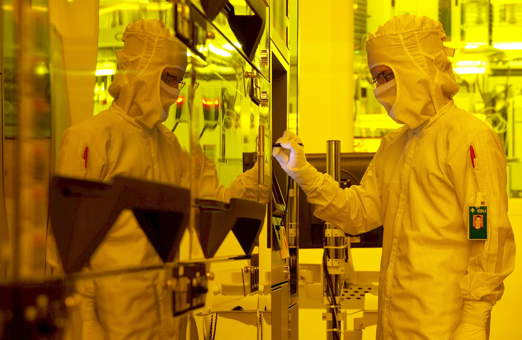
GlobalFoundries, which started to manufacture chips using 14nm low-power early (14LPE) manufacturing technology several months ago, said on Friday that its yields exceed its original expectations. One of the world’s largest contract makers of semiconductors does not reveal its actual 14nm volumes, but since the chips are made for customers, they should meet demands of the latter.
FOLLOW UP: GlobalFoundries: We started to tape-out chips using second-gen 14nm process technology.
GlbalFoundries: 14nm yields are great
“Our 14nm FinFET ramp is exceeding plan with best-in-class yield and defect density,” said Jason Gorss, senior manager of corporate and technology communications at GlobalFoundries. “The early-access version of the technology (14LPE) was qualified in January and is well on its way to volume production, meeting yield targets on lead customer products.”
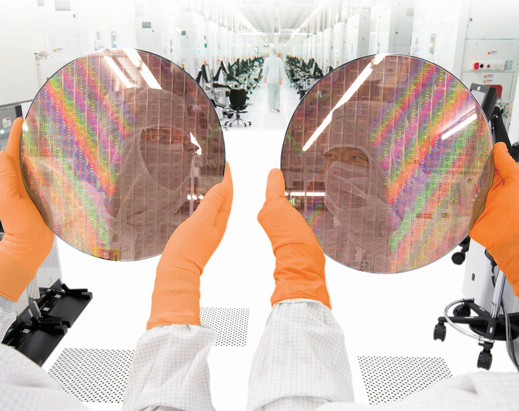
Earlier this year GlobalFoundries indicated that its 14LPE yields were on par with its partner Samsung Foundry (the original developer of the 14LPE), which uses the technology to produce its Exynos 7420 system-on-chip at its fab in Austin, Texas. The SoC is used inside Samsung’s Galaxy S6, S6 Edge and S6 Edge+ smartphones. So far, Samsung has shipped tens of millions of smartphones based on the Exynos 7420 application processor, which indirectly indicates rather good yields of the 14nm process technology.
Another major client for Samsung's 14nm FinFET LPE is Apple, whose A9 system-on-chip for the iPhone 6s and the iPhone 6s Plus will be made using the fabrication process. Analysts expect Apple to sell 80 – 90 million new iPhones by the end of the year.
Working to make 14nm yields better
GlobalFoundries and Samsung are working together in a bid to improve yields and further decrease defect density of the 14nm LPE fabrication process. While the two companies do some changes in the process flow, they tend to stay close to the original and each other in order to offer their clients complete design compatibility and performance consistency.
GlobalFoundries claims that there is a special process in place, which resembles Intel Corp.’s “Copy Exactly” methodology. The “Copy Exactly” requires matching equipment configuration, chemical purity, process recipes and a lot of other things.
“A key part of the value proposition of our partnership with Samsung is the ability to offer true design compatibility at multiple fabs,” said Mr. Gorss. “We do this through a fab synchronization process that is very similar to the ‘Copy Exactly’ methodology. Of course, we can and do make changes to our process flow as necessary, but staying close to ‘copy exact' allows us to drive the fastest possible ramp of the technology.”
Volumes unknown
GlobalFoundries does not reveal how many wafers it processes using the 14nm fabrication technology now, but earlier this year the company indicated that a significant portion of equipment needed for commercial production of chips using 14nm FinFET process had been installed.
It is unclear what equipment GlobalFoundries uses to make 14nm chips at its Fab 8, but originally the semiconductor fabrication plant was allegedly equipped with ASML’s Twinscan NXT:1950i lithography machines. Earlier this year the company acquired new tools specifically to produce chips using newer process technologies (the list probably included lithography tools, metrology tools and a number of other things). GlobalFoundries does not reveal details about its equipment, but the best scanners it could buy in late 2014 or early 2015 were ASML’s Twinscan 1970Ci step-and-scan systems, which can process up to 250 300mm wafers per hour (up from 175wph on the NXT:1950i) and have higher precision than predecessors.
All ASML Twinscan NXT machines use immersion lithography with ultraviolet light at 193nm wavelength. Since modern process technologies are designed for 193nm immersion lithography, semiconductor manufacturers can use all ASML Twinscan NXT machines with some tweaks (to the scanners and other equipment in the fab) to manufacture chips using the latest process technologies. Moreover, all Twinscan NXT scanners are field-upgradeable to the same performance level (but not to the same level of overlay performance) as the latest NXT:1970Ci system.
While the yields of 14LPE seem to be fine, it is unknown how many wafers using the new process technology it can process per month. Theoretically, GlobalFoundries can expand production relatively quickly by upgrading its existing equipment. However, since demands of GF’s clients are unknown, it is uncertain whether it actually needs any upgrades right now. In fact, GlobalFoundries’ main customer – Advanced Micro Devices – reportedly plans to use only more advanced 14LPP [low-power plus] process technology to make its chips sometimes next year.
Discuss on our Facebook page, HERE.
KitGuru Says: It looks like everything is good with 14nm LPE yields at GlobalFoundries and Samsung Foundry. While the Fab 8 upgrade process is not yet finished, it makes a great sense for the chipmaker to wait for ASML’s Twinscan NXT:1980Di to arrive because it can process even more wafers (275wph), thus improving productivity and profitability.

Is this a possibility for the Zen process node or will AMD choose TSMC’s 16nm?
Thanks
apple a9 was made with lpe instead of lpp?
The rumor is just bogus shooting in the dark by some Asian media. Zen is 14nm LPP. I have acquaintances and some former college mates who work for AMD today on the upcoming x86 cores. This isn’t a really a big secret, people put these on their resumes for recruiters and hiring managers to see.
A Way To Get Paid $97/hour And More…….After earning an average of 19952 Dollars monthly,I’m finally getting 97 Dollars an hour,just working 4-5 hours daily online.….. Weekly paycheck… Bonus opportunities…earn upto $16k to $19k /a month……….Only a few hour required to understand and start working///look over here …
.suo……….
➤➤➤http://GoogleTopCareersEarnStandardProfit/get/morethan$97/h…
✥✥✥✥✥✥✥✥✥✥✥✥✥✥✥✥✥✥✥✥✥✥✥✥✥✥✥✥✥✥✥✥✥✥✥✥✥✥✥✥✥✥✥✥✥✥✥✥
lpe
It must be Zen…i mean, what else could AMD be baking on GF’s 14nm? Jim Keller just left, AMD says it will not impact their plans for the coming years..likely meaning Zen’s design is well rounded and ready for manufacturing. Arctic Islands will almost certainly be made at TSMC. K12 was Read’s project, but we have not heard of it since Su. So what else could it be?
Allow me+ to show you a real way to earn a lot of extra money by finishing basic tasks from your house for few short hours a day — See more info by visiting >MY!___@+__ID|
LPE as yields are likely higher; Apple designed for LPE and aren’t under any kind of pressure so have no urgency to change to LPP.
They will likely use 14LPP next year because 10nm will be more expensive due to lower yields and them not being in a rush.